Building better low-light detectors

A stack of alternating layers of GaN and AlN creates an avalanche photodiode with high sensitivity and excellent
controllability
BY LAI WANG, JIYUAN ZHENG, ZHIBIAO HAO AND YI LUO FROM TSINGHUA UNIVERSITY
If you need to measure incredibly low light signals, you have to make a compromise. If you want the best performance, you must select a photomultiplier tube. However, it is fragile and bulky. The alternative, addressing these weaknesses, is the avalanche photodiode (APD), but it is let down by its poor controllability.
The good news, however, is that this lack of controllability will not be plaguing the APD for much longer, thanks to a recent breakthrough by our group at Tsinghua University, working in partnership with researchers at CNRS-CRHEA, France, and the Chinese Academy of Sciences. Together we have developed a novel APD that delivers a record-breaking stable linear gain of over 104 under constant bias "“ that's almost two orders of magnitude higher than that of silicon APDs.
With conventional APDs, producing high multiplication gain requires operation under extremely high bias. When controlled in this manner, there is a drastic rise in the response current, known as "˜breakdown'. This breakdown will not stop until the bias is reduced below its breakdown value.
What this means in practice is that when using an APD, it needs to be periodically quenched below its breakdown bias, with photons only detected when these diodes are under breakdown. It is a compromise between high gain and sustainable detection, and requires the use of complex control circuits. This intrinsic limitation has been plaguing researchers for years, who want an APD that works like a PMT, with a controllable avalanche and the opportunity to operate the device under a simple constant bias with high gain. This is what you get with our device.
It is important to note that avalanche and breakdown are actually two completely different concepts. Breakdown is a compromise, used to ensure that a conventional APD delivers high gain. In this type of device, a significant proportion of the carrier energy that's drawn from the electric field is thermalized by intense scattering. As a result, these diodes have to work under extremely high bias, because this enables electrons and holes to both trigger ionization (see Figure 1(a)). Multiplication proceeds along two opposite directions, forming positive feedback chains that lead to a drastic rise in the response current.
A better approach would be for just one kind of carrier to trigger ionization, leading to an avalanche march in just one direction (see Figure 1 (b)). If that were the case, the avalanche could stop by itself when all the carriers move out of multiplication region. Thanks to this, the APD could provide a suitable response to the signal when it is operated under constant bias, simplifying its use and the accompanying circuitry.
Our device works on this principal, as do several others. In fact, in general, there are three conventional approaches to improving the sensitivity of linear-mode APDs: using materials with a great difference in conduction band and valence band profiles, narrowing the ionization region, and turning to impact ionization engineering.
Figure 1. Unipolar ionization and bipolar ionization. (a) In a unipolar ionization APD, only one kind of carrier can trigger ionizations. Avalanche proceeds unidirectionally. (b) In a bipolar ionization APD, all carriers can trigger ionization. Avalanche proceeds bi-directionally. The solid and hollow circles represent electrons and holes, respectively; and the small and large arrows represent the carrier drifting direction and the avalanche direction, respectively.
With the first of these, suitable materials are silicon, InAs and HgCdTe. For these semiconductors, the first energy valley of the conduction band is very deep, and electrons traversing it can increase in energy, triggering ionizations without inter-valley scattering. This means that the ionized electrons have far higher energies than the holes in this material. In these devices, gain is relatively high "“ but it is not high enough. If the APD is made from silicon, the effective mass for the conduction band is relatively large, inner-valley scattering cannot be ignored, and the efficiency of electron-triggered ionization is not high enough; and if this device is made from InAs or HgCdTe, the narrow bandgap leads to a risk of Zener breakdown, particularly under high electric fields. What's more, the gain is not that high.
The second option, narrowing the ionization region, can be accomplished with the "˜dead space' effect. By localizing the position for ionization, triggering of ionization is restricted to just one type of carrier. There is a price to pay, however "“ limited ionisation time, and ultimately diminished gain.
The third approach is impact ionization engineering, a technique that involves deploying periodic doping layers and heterojunctions. Here, the challenge is that the active region for ionization is so thick that it is hard to grow many cycles. Gain is limited to around 1000.
If commonly used semiconductors are adopted to construct APDs with either a conventional homojunction or an impact ionization engineering architecture, inter-valley scattering disrupts the transport of carriers. This prevents them from hitting the ionization threshold energy, resulting in a low ionization coefficient.
However, it is possible to overcome scattering and realise a high gain with the GaN material system. For both GaN and AlN, there is a deep G valley with a depth of about 2 eV in the first conduction band, and no such valley in the valence band. Due to this, electrons transporting within the G valley of either GaN or AlN experience a relatively weak scattering.
When using GaN to make an APD, the ionization threshold energy for electrons is 5.3 eV. Although this is significantly higher than the depth of the G valley, the conduction band offset between GaN and AlN is 2 eV. So, when electrons travel from GaN to AlN, along the (0001) direction, they enter into the G valley of AlN and are given an increase in energy to more than 4.0 eV. As this is quite close to the ionisation threshold, only moderate electric fields can trigger ionization impact.
We are pioneering the development of this APD architecture, using a GaN/AlN periodically stacked structure to realize controllable electron multiplication (see Figure 2 (a) for the bandstructure of our device). To kick-start this effort, we used Monte Carlo simulations based on first-principle theory to model the behaviour of both a conventional GaN-based heterojunction APD and our novel variant "“ it has a periodic structure, containing alternating AlN and GaN layers with a thickness of 10 nm.
Figure 2. (a) Applying a relatively weak field to an APD with
a periodically stacked GaN/AN structure allows electrons to reach the
ionisation threshold of 5.3 eV. (b) Transmission electron microscopy reveals
the high quality of this MBE-grown structure.
Simulations suggest that our new device delivers a tremendous hike in the ionization coefficient for electrons, while realising a negligible increase for holes. When the electric field exceeds 2.8 MV/cm, the electron ionization saturates at around 3.96à—105 cm-1. Under these conditions, the probability of electron-triggered ionization within each 20 nm-thick GaN/AlN period is nearly 80 percent. Such a high ionization coefficient has never been realized in APDs with either heterojunction or impact ionisation engineering structures.
To validate the capability of this APD, we have built a prototype that features 20 periods of 10 nm-thick GaN and AlN layers. This replaces the conventional multiplication layer in a GaN-based, p-i-p-i-n device with separate absorption and multiplication regions.
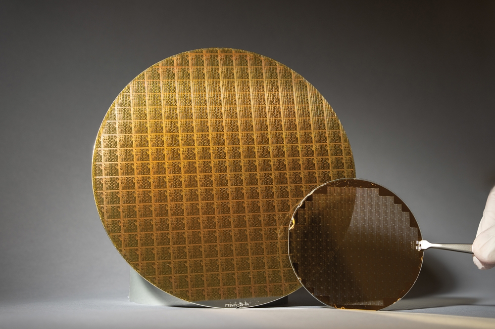
A Riber 32 P MBE reactor was used to grow this structure on a 2-inch, c-plane template produced by Suzhou Nanowin Science and Technology. On this foundation, a 4 mm-thick AlN layer on sapphire, we grew a 50 nm-thick AlN layer, followed by a silicon-doped 500 nm-thick GaN layer, 20 periods of GaN (10 nm) and AlN (10 nm), a magnesium-doped 10 nm-thick GaN layer, a 300 nm-thick non-intensively-doped GaN layer and 100 nm-thick magnesium-doped GaN. Cross-sectional transmission electron microscopy reveals that the layers are uniform, with a thickness that coincides with the designed value (see Figure 2 (b)).
To prevent edge leakage and breakdown, we create a double-mesa architecture, using inductively-coupled-plasma, dry etching. The mesa has an outer diameter of 35 mm, and an inner diameter of 25 mm that provides the light absorption surface. A layer of SiO2 is added by plasmas-enhanced CVD to passivate the device. A p-type transparent ohmic contact is formed from Ni (2.5 nm)/Au (8 nm), and an n-type ohmic contact is created with Cr (25 nm)/Au (200 nm). A 100 nm-thick layer of gold provides the electrode pads that complete device fabrication (see Figure 3 (a)).
We have evaluated the performance of our APDs by measuring current-voltage curves, in the dark and under illumination, with an Agilent Type 4155C semiconductor analysis meter. Illumination of the front of our chip comes from a 350 nm source, with emission from a xenon lamp directed through a monochromator. The light power density is 51 mW/cm2, equating to 250 pW of power coupled into the chip.
Unlike conventional APDs, the external quantum efficiency of our device increases steadily with bias voltage (see Figure 3 (b)). Gain saturates at 1à—104. This number can be expressed as about 214, implying that photon-generated electrons are repeatedly multiplied at least 14 times during a single-pass transport. From this data we can determine that the probability for electron-triggered ionization at each period of the APD is about 70 percent. This is quite close to the simulation result of 80 percent at the saturation electric field.
To confirm that our APD can work under constant bias with high gain, we have recorded the room-temperature response under a constant bias of 65 V (see Figure 3(c)). This current responds well with the switching on and off of the incident ultraviolet light, while the external quantum efficiency hits 104. This result showcases the superiority of our APD, as conventional devices working under constant bias cannot reach such high gain.
Figure 3. (b) The GaN/AlN periodically stacked APD features a double-mesa design. (b) I-V curves and external quantum efficiency (EQE) of the device. (c) Response of the device under constant bias. (d) Excess noise of the APD under different values of gain.
This collection of results demonstrates that electron-triggered ionisation in our GaN/AlN APDs is highly-efficient and controllable. What's more, even better performance is possible. Since the electron ionization coefficient is extremely high, and the multiplication performance is determined by the number of GaN/AlN stacks, simply increasing the number of periods of GaN and AlN, or optimising their thicknesses, should yield a higher gain. An additional insight into the workings of the APD is provided by analysing excess noise (see Figure 3 (d)). Evaluating the ionization coefficient ratio k, by comparing the excess noise with data calculated by the VanVliet/Matsuo model, using different fitting parameters of k, shows that ionization originates purely from electrons "“ that conclusion can be drawn, because the excess noise factor fits well with the curve for a value of k of zero, when the gain is below 100.
For a gain that is higher than 100, there is a slight feedback from holes during the ionization process. However, even when the gain is as high as 10,000, the value of k is still just 0.05, which is comparable to the value for a silicon APD working under linear mode. That's not to say, however, that performance is similar: our APDs deliver a better linear performance, because their gain is over 10,000, while for silicon it is only about 100. When gain is 10,000, the excess noise factor is only 500.
Our results are very encouraging for the future of low-light signal measurements. They show that there will come a time when there is no need to select between fragile, bulky photomultiplier tubes and APDs that are difficult to control, thanks to our development of high-performance, periodically stacked structures based on the pairing of AlN and GaN.


