
Making more efficient, more reliable millimetre-wave HEMTs
Miniaturized HEMTs equipped with ultra-thin barriers and high-quality passivation enable record-breaking efficiencies in the Q-band
BY KATHIA HARROUCHE, RIAD KABOUCHE AND FARID MEDJDOUB FROM IEMN
FOR RF SYSTEMS, a great deal is gained by going to higher frequencies. To draw on this, during the coming years much effort will be devoted to rolling out next-generation 5G networks, satellite communications and radar systems operating at millimetre-wave frequencies. Moving to this domain satisfies the demand for higher bandwidth, while facilitating higher data transmission rates.
MMICs are now capable of operating at millimetre-wave frequencies, thanks to recent, ongoing progress in device fabrication and processing. When made from silicon, this delivers a few watts below the Ka-band but struggles to produce sufficient power at higher frequencies. Overcoming this weakness is the GaN-based HEMT, a device delivering a strong performance from a small size, thanks to its great material properties that include a wide bandgap, a high electron mobility and high saturated-electron velocity. Armed with all these attributes, GaN-based RF power devices have positioned themselves as ideal building blocks for making MMICs, as they enable a hike in the output power of compact solid-state power amplifiers, so that they can serve more applications.
When deployed in solid-state power amplifiers, a critical parameter for the GaN HEMTs is its power-added efficiency (PAE) – this directly affects its power dissipation. One of the key goals facing developers of GaN HEMTs is to maximise PAE, so that the device can deliver a high output power density (POUT) in the millimetre-wave range.
In addition to delivering high performance in this domain, GaN-based MMICs must combine robustness with reliability if they are to enjoy success in high-volume applications. Much more work is needed on this front, given that there are very few published reports related to millimetre-wave GaN device reliability. Efforts will need to be directed at scaled material and devices, as this will enable demonstration of high stability, reproducibility and uniformity.
Ultrathin barriers
The tried-and-tested pathway for enhancing the RF performance of semiconductor devices is to scale down transistor dimensions. For GaN HEMTs, this must go hand-in-hand with optimisation of the epilayer stack, especially the top barrier layer. Emerging ultrathin barrier heterostructures, such as AlN/GaN, are a promising architecture for the millimetre-wave range, because they offer the possibility to highly scale the epitaxial structure while retaining the benefits associated with high polarization, such as a high current density.
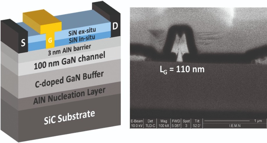
Figure 1: Schematic cross section of an AlN/GaN HEMT (left) and a focused ion-beam view of a 110 nm T-gate (right)
By adopting this approach, our team from the Institute of Electronics, Microelectronics and Nanotechnology in Villeneuve-d’Ascq, France, has broken the record for PAE at 40 GHz. Crucial to our success has been our collaboration with Soitec-Belgium, the division created through the acquisition of EpiGaN. This partner of ours, an expert in MOCVD of III-Ns, has provided us with high-quality AlN/GaN heterostructures.
We have fabricated our AlN/GaN HEMTs from epiwafers that feature a SiC substrate and a 3 nm-thick AlN barrier. These devices have a 110 nm T-shaped gate and are capped with a dual purpose 10 nm-thick SiN layer that is grown in-situ: it provides early passivation, while reducing trapping effects (see Figure 1 for a cross-sectional diagram of our transistor (a), and a focused ion beam view of the gate (b)).
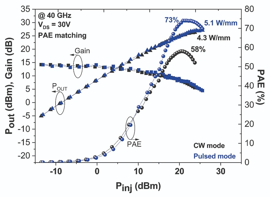
Figure 2. CW and pulsed power performances at 40 GHz of a 3 nm AlN/GaN HEMT 2×50 μm with LG = 110 nm and LGD = 0.6 μm at VDS = 30 V.
Note that the traditional approach for increasing the aspect ratio is to apply the so-called gate-recess. This brings the gate closer to the channel regardless of barrier thickness, often at the expense of irreversible damage to the crystalline material that leads to serious reliability issues.
A significant threat from downscaling is that it hampers device robustness, a crucial concern for all applications. For ultrashort transistors operating at high drain voltages – they are typically more than 15 V – there is a need for high device reliability and low trapping effects. To excel on both fronts, there need to be high quality material and processing. Both goals can be accomplished by reducing defect density and enhancing surface robustness through the inclusion of an in-situ SiN cap layer.
Q-band efficiency records
To increase the efficiency of millimetre-wave GaN HEMTs that operate at a high output power density while maintaining strong device robustness, there needs to be an increase in surface stability under a high electric field. We accomplish this by combining optimised processing with the incorporation of an in-situ SiN cap layer. Our approach to realising this has been continuously refined over many years, with improvements including reductions in gate resistance and parasitic capacitances. We select a gate-to-drain distance of 0.6 μm, which provides the ultimate trade-off between RF performance and breakdown voltage.
Large signal characterization of our HEMTs reveals outstanding power performances at 40 GHz.
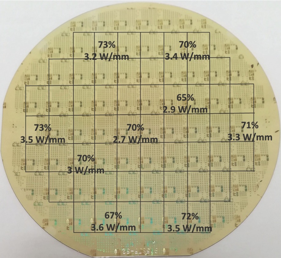
Figure 3. Manuel mapping of 40 GHz pulsed large signal performances at a VDS of 20 V of the 3 nm AlN/GaN wafer with LG = 110 nm and LGD = 0.6 μm (PAE matching).
Our 4-inch wafers have excellent yield and uniformity, according to manual mapping measurements made on a significant proportion of our HEMTs. Measurements at 40 GHz on 2×50 μm transistors with a 110 nm gate length and a gate-to-drain distance of 0.6 μm show that for a drain-source voltage of 20 V, PAE is typically 70 percent and POUT 25 dBm. This is a power performance combination that sets a new benchmark in the Q-band.
Increasing the RF performance of the GaN HEMT increases its commercial appeal, but if it is to enjoy market success, it also requires proven reliability. This is the biggest challenge for GaN HEMTs with gate lengths below 150 nm, because compared with qualified GaN technologies, they have a significantly higher electric field peak, and consequently, a high junction temperature under high drain bias.
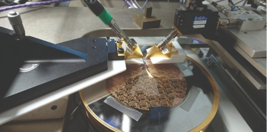
Active load pull measurements at 40 GHz.
We attribute increased robustness to the higher structural quality of the ultrathin barrier layer and/or the in-situ SiN cap layer interface. This has led to an increase in the safe operating area under harsh conditions.
W-band promise
There is growing interest in the W-band, which offers shorter wavelengths and wide frequency bands. Within the W-band, used to conquer new fields of science and industry, is an atmospheric transparency window at 94 GHz that allows for imaging millimetre-wave radar. The 94 GHz frequency also has the potential to be employed for a number of applications associated with defence, astronomy and security.
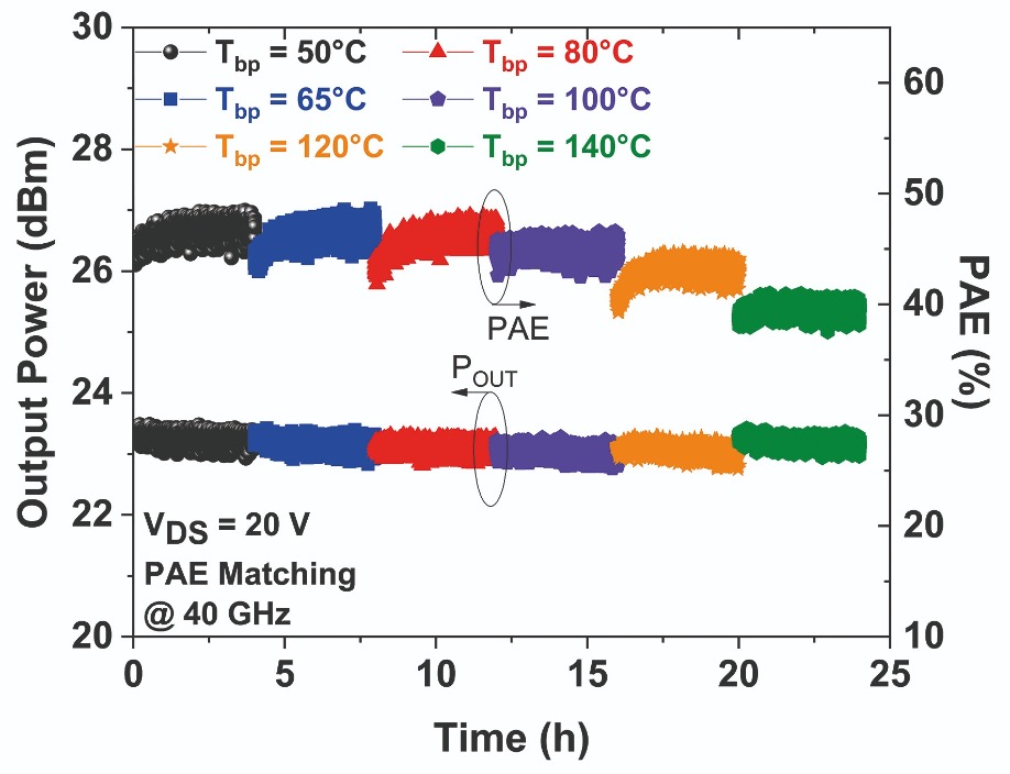
Figure 4. CW output power and PAE monitoring for 24 hours at several base plate temperatures up to 140°C with VDS = 20 V (PAE matching) of a 3 nm AlN barrier HEMT.
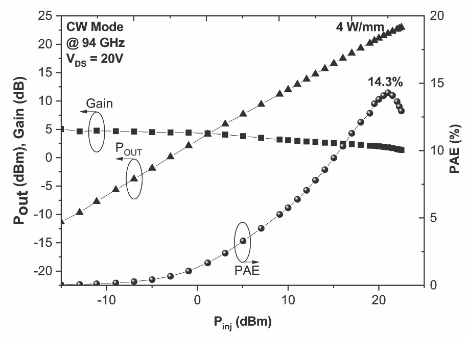
Figure 5. CW power performances at 94 GHz of an AlN/GaN HEMT 2×25 μm with LG = 110 nm for LGD = 0.6 μm at VDS = 20 V.
The results obtained at various frequencies demonstrate a very promising pathway to realising efficient, robust GaN HEMTs all the way to 100 GHz. However, while we are encouraged by a PAE above 70 percent in the Q-band, and the accompanying short-term reliability at high temperatures, we acknowledge that there is still much work to do. There is a need to demonstrate state-of-the-art performance at the MMIC level, alongside long-term reliability – that must include monitoring that lasts for several-thousand hours. Another direction worthy of attention is to investigate refining the heterostructure to further decrease trapping effects. Succeed in this endeavour, and the door could open to an even larger number of applications involving GaN HEMTs operating in the millimetre-wave.


