
InP empowers phased-array radar
Delivering record efficiencies in the Q-band, MMICs made from InP HBTs are the ideal choice for phased-array radar
BY ANDREA ARIAS-PURDUE, PETRA ROWELL, MIGUEL URTEAGA, KEISUKE SHINOHARA, ANDY CARTER AND JOSH BERGMAN FROM TELEDYNE SCIENTIFIC AND IMAGING AND KANG NING, MARK RODWELL AND JAMES BUCKWALTER FROM THE UNIVERSITY OF CALIFORNIA AT SANTA BARBARA
THE DEVELOPMENT of radar can be traced back as far as the late nineteenth century, to a time when German physicist Heinrich Hertz first demonstrated the reflection of radio waves by metallic objects. Exploiting this observation, engineers in the early twentieth century built a growing number of radar systems. While representing a staggering achievement, this traditional design has its downsides: it is bulky; and it takes time to re-orientate the direction of the beam, due to mechanical steering.
Addressing these weaknesses is the more recent phased-array radar, which features electronic synthesis of the beam. By adjusting the phase of the signal transmitted out of each element, it is possible to dial in the desired radiation pattern.
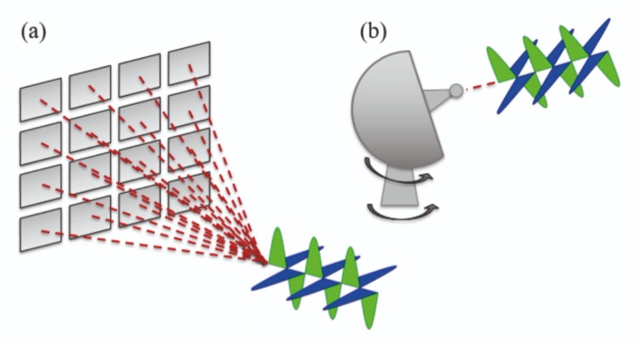
Figure 1. A 16-element phase-arrayed radar (a) and a conventional mechanically steered radar (b).
Lying at the heart of a phase-arrayed radar are full receiver and transmitter units, each equipped with an RF amplifier and antenna. First-generation units were constructed with silicon-based technology – more than a decade ago a team from Caltech broke new ground by demonstrating silicon-based phased array receivers with 8 elements, operating at 24 GHz.
However, more recently, due to demand for phased-array radar operating in the millimeter-wave – that is, above 30 GHz – new materials have been introduced, to cater for greater demands placed on the chip technology. As the frequency increases, the size of the chip must shrink, due to considerations associated with the element spacing due to the shorter wavelength of the radar technology. This leads to the need for a higher RF output power density per unit chip, and a high efficiency that ensures a safe semiconductor device operating junction temperature and ultimately reliable operation.
The key to meeting all these criteria is to switch from using silicon-based devices to those based on III-Vs. At frequencies above 30 GHz, compound semiconductor devices are setting new benchmarks for: power density, judged in terms of Watts per chip area; raw power, measured in Watts; and efficiency for a given bandwidth. It is for this reason that our team from Teledyne Scientific and Imaging are developing phased-array technology based on InP HBTs, which we have used to make MMICs operating at 47 GHz with record power-added efficiency (PAE). We have selected this particular III-V because it has a high carrier mobility, and a higher bandgap than silicon and SiGe, attributes that enable high-voltage handling and a very high power gain at microwave frequencies – amongst the highest for any semiconductor system.
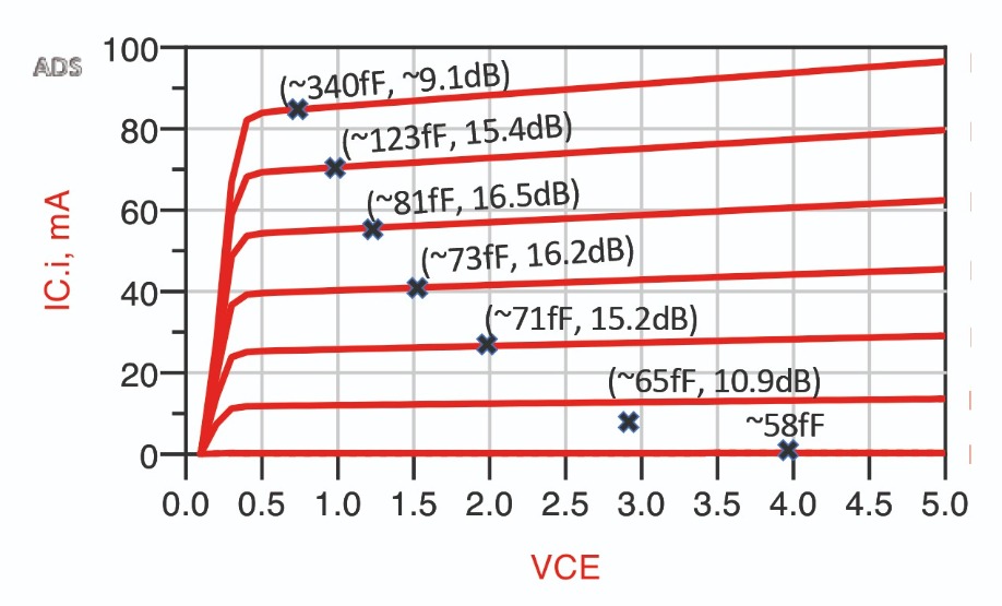
Figure 2. Simulated output current-voltage (I-V) curves of 10 μm2 common emitter power cell, along with effective output capacitance and MAG at selected loadline bias.
To evaluate the suitability of our InP technology for millimetre-wave power amplifiers, we have undertaken load-pull simulations. They involved simulating a single-stage amplifier, varying the load and source impedances, and, at each impedance pair, sweeping the RF input power and plotting the device response. Using this approach, we obtained values for output power, DC power, gain, and efficiency.
Our load-pull simulations indicate that our InP HBTs should produce an excellent peak PAE and associated RF output power across very wide bandwidths (see Figure 3). Note that the results that we report correspond to the fixed source and load impedance shown therein, which offered the best peak PAE across 24 GHz to 60 GHz, based on load and source-pull simulations. Great performance in this domain bodes well for millimetre-wave radar.
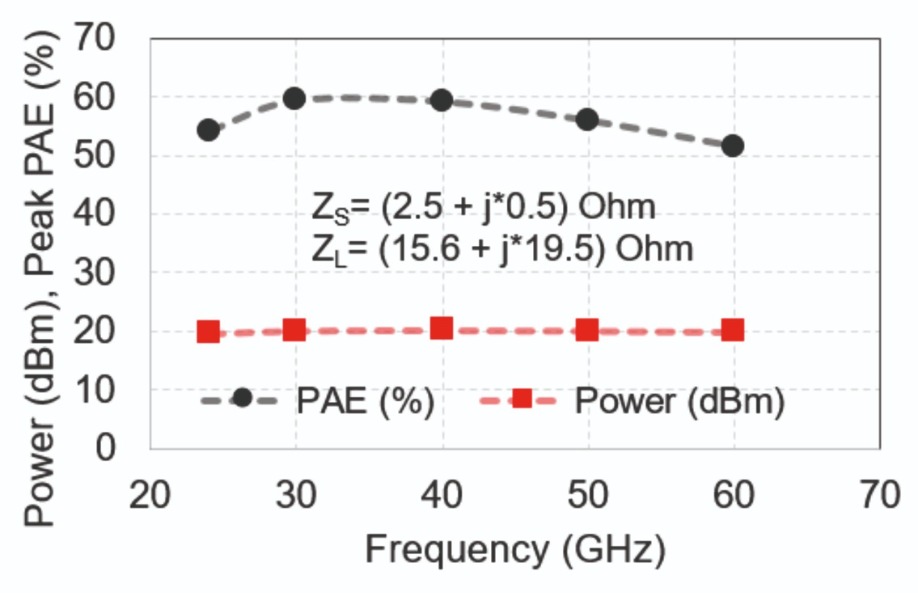
Figure 3. Load pull simulations results (power and PAE) at fixed source and load impedance of 20 dBm InP HBT power cell.
Based on our promising results, we selected this device, which is a common-emitter power cell with a total emitter periphery of 15 μm2, as the key building block for producing an amplifier operating in the Q-band. We targeted an RF output power of 100 mW, for frequencies of 45 GHz to 47 GHz. For this amplifier, we decided to use a device bias point of 3.2 mA μm-2, because this offers the best combination of output power and peak PAE.
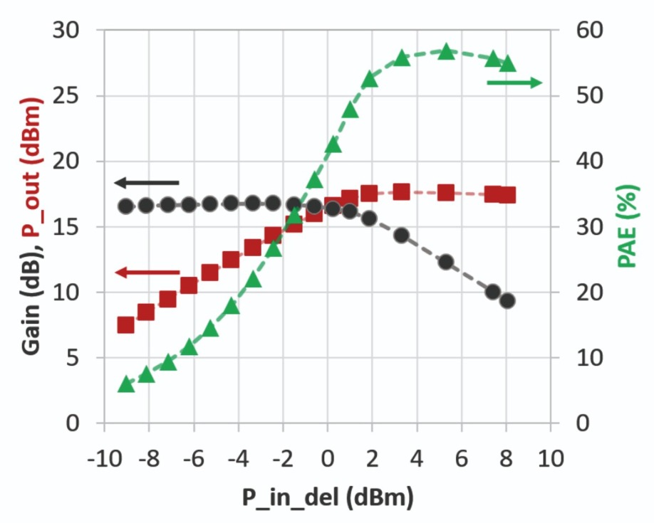
Figure 4. Load pull measurements of designed power cell (15 μm2). Measurements were made using an optimum gamma GLOAD of 0.6 / 120°
One can see our implementation of meandered microstrip lines in an optical image of our chip, shown in Figure 5. It is very compact design, with an inner area of 276 x 600 μm2, which includes DC blocking and bypass capacitors. Including RF pads, the total area of our MMIC chip is 0.185 mm2.
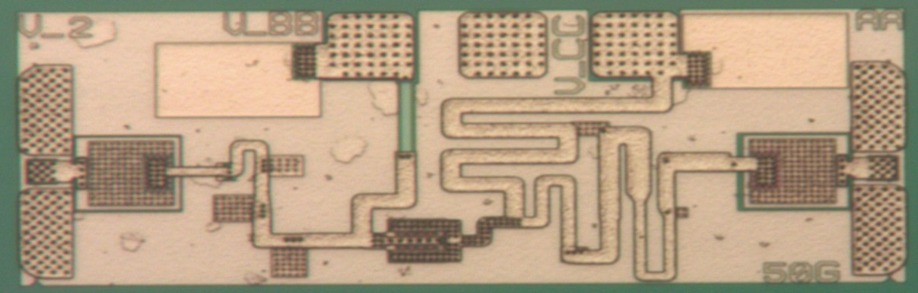
Figure 5. Micrograph of a fabricated InP HBT PA.
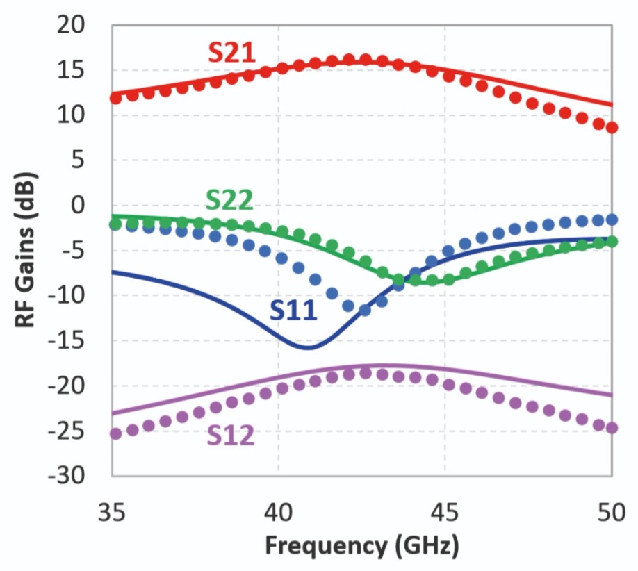
Figure 6. PA small signal response at VCC= 2.75 V, VBB=2.35 V (IC,Q = 47 mA). The solid lines correspond to simulated performance while the symbols correspond to the measured response.
At 47 GHz, the frequency with the highest collector efficiency, the PAE is a record-breaking 46 percent, and the output power 119.7 mW. This is well above our 100 mW target, and if this chip were to be deployed in a phased-array radar, it would enable a 40 dBm effective isotropic radiated power for the 8-element array, given an antenna gain of 4 dBi, requiring 18 dBm per transmitter element. Note that at 47 GHz, the PAE reached is above 40 percent at the 1dB compression point, highlighting its high efficiency at back-off for applications where linearity is important, and thus power back-off from saturation is required.
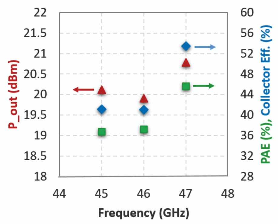
Figure 7. Summary of measured power performance at 45 GHz, 46 GHz and 47 GHz.
GaN, which is widely championed as by far the best material for making great RF devices, does deliver a high power, but compared to our InP MMIC, power gain is significantly lower and PAE slightly lower. Offering similar RF power levels to our chip is the SiGe HBT, but it operates at a lower efficiency.
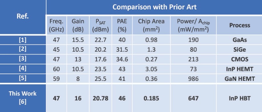
Table 1. Comparison of the results obtained in this work to prior art. [1] G. Lv et al. IEEE Microw. Wirel. Compon. Lett. 28 530 (2018). [2] K. Datta et al. “A 20 dBm Q-band SiGe Class-E power amplifier with 31% peak PAE,” Proceedings of the IEEE 2012 Custom Integrated Circuits Conference, San Jose, CA, 2012, pp. 1-4.A. [3] Chakrabarti et al. “High power, high efficiency stacked mmWave Class-E-like power amplifiers in 45nm SOI CMOS,” Proceedings of the IEEE 2012 Custom Integrated Circuits Conference, San Jose, CA, 2012, pp. 1-4. [4] S. M. J. Liu et al. “High efficiency monolithic InP HEMT V-band power amplifier,” GaAs IC Symposium. IEEE Gallium Arsenide Integrated Circuit Symposium. 21st Annual. Technical Digest 1999 (Cat. No.99CH36369), Monterey, CA, USA, 1999, pp. 145-147. [5] M. Micovic et al. IEEE Electron Dev. Lett. 38 1708 (2017) [6] A. Arias-Purdue et al. “A 120-mW, Q-band InP HBT Power Amplifier with 46% Peak PAE,” 2020 IEEE/MTT-S International Microwave Symposium (IMS), Los Angeles, CA, USA, 2020, pp. 1291-1294
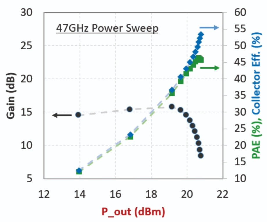 Figure 8. Measured power sweep at 47 GHz, at VCC= 2.75 V and VBB= 2.35 V (IC,Q= 47 mA).
The authors acknowledge Teledyne Scientific’s support through IRAD. The authors also acknowledge Teledyne’s Fabrication Operations group for the MMIC fabrication.
K. Brown et al. “7kW GaN W-band transmitter,” 2016 IEEE MTT-S International Microwave Symposium (IMS), San Francisco, CA, 2016, pp. 1-3.
Z. Griffith et al. “71–95 GHz (23–40% PAE) and 96–120 GHz (19–22% PAE) high efficiency 100–130 mW power amplifiers in InP HBT,” 2016 IEEE MTT-S International Microwave Symposium (IMS), San Francisco, CA, 2016, pp. 1-4.
M. Urteaga et al. “InP HBT Integrated Circuit Technology for Terahertz Frequencies,” 2010 IEEE Compound Semiconductor Integrated Circuit Symposium (CSICS), Monterey, CA, 2010, pp. 1-4.
A. Arias-Purdue et al. “A 120-mW, Q-band InP HBT Power Amplifier with 46% Peak PAE,” 2020 IEEE/MTT-S International Microwave Symposium (IMS), Los Angeles, CA, USA, 2020, pp. 1291-1294, doi: 10.1109/IMS30576.2020.9223945.


