
HKUST researchers extend the scope of GaN
Introducing complementary logic circuitry into the family of wide-bandgap GaN electronics
A research team led by Kevin Chen of Department of Electronic and Computer Engineering at The Hong Kong University of Science and Technology (HKUST) has recently inducted a new member, the complementary logic circuitry, into the family of wide-bandgap GaN electronics, thereby substantially extending the horizon of the GaN research realm. The functionality and performance of GaN-based electronic devices and integrated circuits are expected to be further improved and become more competitive.
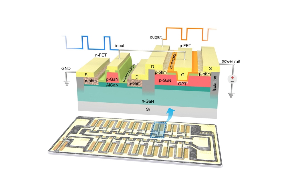
Development of the energy-efficient GaN CMOS technology has been slow until recently, as hindered by the difficulties in implementing p-channel transistors and integrating them with complementary n-channel ones.
On a GaN power device technology platform, Chen’s team developed a new approach to tackle a notorious problem associated with the gate-dielectric/channel interface. They engineered a “buried channel” structure enabled by an oxygen plasma treatment (OPT) technique, consequently realizing p-channel GaN transistors with well-balanced performance matrix of threshold voltage for enhancement-mode operation, high ON/OFF current ratio, and high current driving capability. Monolithic integration process was also developed to realize GaN CMOS ICs that are seamlessly integrated with GaN power switching devices.
The team says it has demonstrated a complete set of GaN CMOS-based elementary logic gates including NOT, NAND, NOR gates, and the transmission gate. The team also demonstrated multiple-stage logic circuits that can be operated at megahertz frequencies. “This is an exciting leap forward. We have first proven that all building blocks are functional, then these building blocks could be put together for more complicated entities. Therefore, any GaN-based complementary logic circuits can be constructed by making combinations of these logic gates,” says Chen.
The device technology in the work was developed at HKUST’s Nanosystem Fabrication Facility (NFF) on Clear Water Bay campus. The work is partially supported by a Hong Kong RGC Research Impact Fund (RIF) project and has recently received funding support from Shenzhen-Hong Kong-Macau Science & Technology Program. This work has recently been published in Nature Electronics.
'Gallium nitride-based complementary logic integrated circuits' by Zheyang Zheng et al; Nature Electronics volume 4, 2021


