
Army research develops novel near-field Thermo-PV system
InGaAs-based thin film photovoltaic cells could efficiently turn thermal energy into electricity for soldiers
Army-funded research has demonstrated a new approach to turning thermal energy into electricity that could provide compact and efficient power for soldiers on future battlefields.
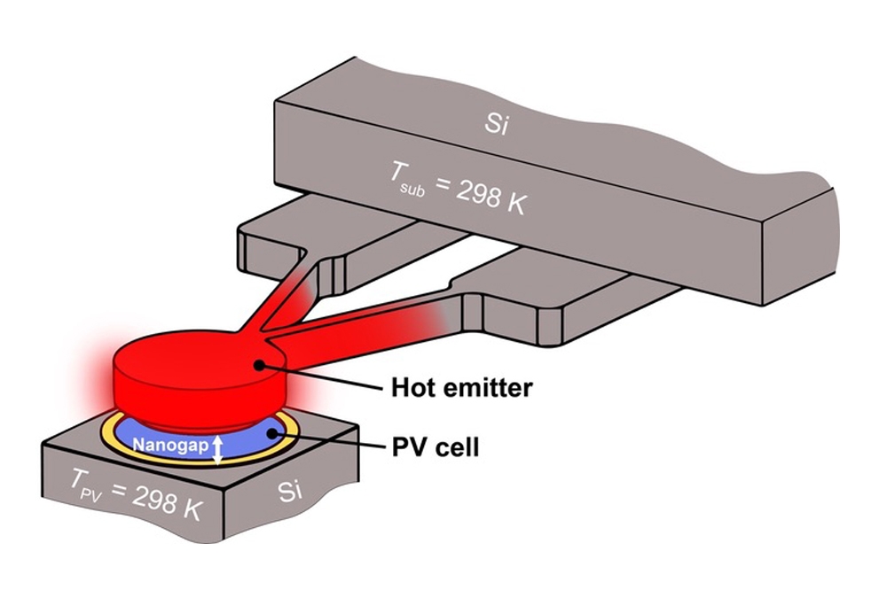
Hot objects radiate light in the form of photons into their surroundings. The emitted photons can be captured by a photovoltaic cell and converted to useful electric energy. This approach to energy conversion is called far-field thermophotovoltaics, or FF-TPVs, and has been under development for many years; however, it suffers from low power density and therefore requires high operating temperatures of the emitter.
The research, conducted at the University of Michigan and published in Nature Communications, demonstrates a new approach, where the separation between the emitter and the photovoltaic cell is reduced to the nanoscale, enabling much greater power output than what is possible with FF-TPVs for the same emitter temperature.
This technique exhibited a power density almost an order of magnitude higher than that for the best-reported near-field-TPV systems, while also operating at six-times higher efficiency, paving the way for future near-field-TPV applications, according to Edgar Meyhofer, professor of mechanical engineering, University of Michigan.
“The Army uses large amounts of power during deployments and battlefield operations and must be carried by the Soldier or a weight constrained system,” said Mike Waits, US Army Combat Capabilities Development Command’s Army Research Laboratory. "If successful, in the future near-field-TPVs could serve as more compact and higher efficiency power sources for Soldiers as these devices can function at lower operating temperatures than conventional TPVs.”
The efficiency of a TPV device is characterised by how much of the total energy transfer between the emitter and the photovoltaic cell is used to excite the electron-hole pairs in the photovoltaic cell. While increasing the temperature of the emitter increases the number of photons above the band-gap of the cell, the number of sub band-gap photons that can heat up the photovoltaic cell need to be minimised.
“This was achieved by fabricating thin-film TPV cells with ultra-flat surfaces, and with a metal back reflector,” said Stephen Forrest, professor of electrical and computer engineering, University of Michigan. “The photons above the band-gap of the cell are efficiently absorbed in the micron-thick semiconductor, while those below the band-gap are reflected back to the silicon emitter and recycled.”
The team grew thin-film InGaAs photovoltaic cells on thick semiconductor substrates, and then peeled off the very thin semiconductor active region of the cell and transferred it to a silicon substrate.
All these innovations in device design and experimental approach resulted in a novel near-field TPV system.
“The team has achieved a record ~5 kW/m2 power output, which is an order of magnitude larger than systems previously reported in the literature,” said Pramod Reddy, professor of mechanical engineering, University of Michigan.
Researchers also performed theoretical calculations to estimate the performance of the photovoltaic cell at each temperature and gap size and showed good agreement between the experiments and computational predictions.
“This current demonstration meets theoretical predictions of radiative heat transfer at the nanoscale, and directly shows the potential for developing future near-field TPV devices for Army applications in power and energy, communication and sensors,” said Pani Varanasi, program manager, DEVCOM ARL that funded this work.
'Near-field thermophotovoltaics for efficient heat to electricity conversion at high power density' by Rohith Mittapally et al; Nature Communications volume 12 (2021)


