
Boosting GaN blocking voltages
A sputtered layer of p-type NiO nearly doubles the blocking voltage of GaN-on-silicon Schottky barrier diodes
Engineers from EPFL, Switzerland, are claiming to have broken the record for the breakdown voltage of GaN-on-silicon Schottky barrier diodes. The team’s devices, featuring a p-type NiO layer that acts a junction termination extension, are capable of blocking up to 443 V.
Junction termination extensions are common structures, widely deployed in silicon and SiC devices to prevent localised peaking of the electric field and ultimately ensure a higher blocking voltage.
However, in those devices the junction termination extensions are formed by implantation or diffusion, to create selectively doped regions. With GaN, ion implantation is still in its infancy, requiring pressures of more than 1 GPa and temperatures above 1200degC.
To side-step issues associated with ion implantation, the researchers at EPFL, led by Elison Matioli, have switched to RF sputtering of NiO, a p-type conductive oxide that can realise high hole densities. Note that in 2020, researchers at Nanjing University and at Sun Yat-sen University both reported the use of doped NiO to realise a high reverse-blocking voltage in Ga2O3, despite the large band offset between these two materials. “This inspired us to evaluate the use of p-NiO as junction termination extensions for GaN power devices,” says Matioli.
He and his co-workers are not the first to report the addition of p-NiO junction termination extensions to GaN Schottky barrier diodes. Earlier this year, a team led by researchers at Tokushima University, Japan, announced the fabrication of devices with this architecture. Using bulk GaN substrates and a 14µm-thick drift layer, they realised a blocking voltage of less than 250 V.
The higher blocking voltage is likely to partly result from the switch from a TiN anode that has a Schottky barrier height of 0.6 eV to a nickel anode with a height of 0.9-1 eV. There may also be differences in the design and fabrication of the diodes. “We spent a considerable amount of time optimising the design of the junction termination extension, the deposition conditions of p-NiO, as well as perfecting the fabrication process for our device,” says Matioli.
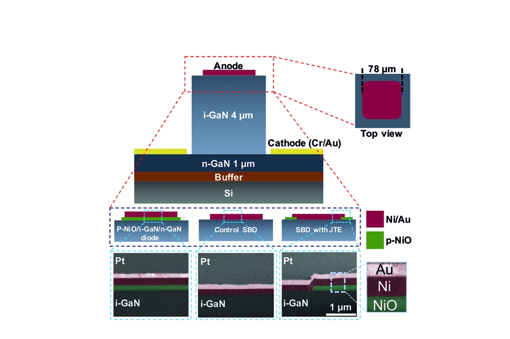
The team’s devices were fabricated from 150 mm GaN-on-silicon epiwafers, provided by Enkris. These epiwafers had a 1.1µm-thick buffer, followed by a 1 µm-thick layer of n-type GaN and a 4 µm-thick layer of intrinsic GaN. At EPFL, engineers added a 160 nm-thick layer of NiO by RF sputtering, before using a lift-off process to define the junction termination extension region. To complete diode fabrication, the engineers used Ni/Au to form a p-type ohmic contact, before creating a mesa with reactive-ion etching that enabled access to the n-type layer – this facilitated the addition of Cr/Au to create an n-type ohmic contact.
Current-voltage measurements on a conventional GaN Schottky barrier diode, grown as a control, and the variant with the junction termination extension, show that this modification does not have a significant impact on the on-resistance or the turn-on voltage. However, the blocking voltage has a substantial increase, rising from 230 V to 443 V.
The team is aiming to make additional improvements to its p-NiO deposition conditions. Efforts will focus on RF sputtering power and ambient gas flux, as this could reduce the reverse leakage current at the p-NiO/GaN interface. “This will help us achieve a variety of devices, like merged p-i-n Schottky diodes, junction barrier Schottky diodes, as well as JFETs,” says Matioli.
Pictured above are the three variants of the diode were produced: one with a p-NiO layer, to enable study of transport properties; a control; and a Schottky barrier diode (SBD) with a junction termination extension (JTE). Focused ion-beam cross-sectional scanning electron microscopy images of the regions are depicted in the blue boxes.
Ref
R. Khadar et al. Appl. Phys. Express 14 071066 (2021)


