
$4.4M grant to develop next-gen night vision technology
US Navy grant will advance sensor technology using the semiconductor silicon germanium tin
University of Arkansas researchers have received a $4.4 million award from the US Office of Naval Research to develop the next generation of infrared sensors used in night vision technology.
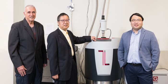
The three U of A researchers (pictured above L to R ) — distinguished professor Greg Salamo, electrical engineering professor Shui-Qing Yu, and Jin Hu, assistant professor of physics — will collaborate with the Navy Surface Warfare Research Center, Crane Division, and Arktonics, a local company.
Together, they will use the semiconductor silicon germanium tin in designing and building the prototype of a superior and less-expensive infrared camera. The military uses infrared imaging technologies for night vision technology.
The grant will pay for specially designed equipment that will help the team develop the infrared imaging sensor array made of silicon germanium tin. The team will then integrate this array with a complementary metal oxide semiconductor, known as CMOS, on the same chip. CMOS technology is used for making integrated-circuit chips for microprocessors, controllers and other digital and analog circuits, including image sensors. The combination is more effective at harnessing ambient light, an essential element in night vision technology.
Current technologies rely on semiconducting alloys such as mercury cadmium telluride and other material-based photodetectors. These alloys have several limitations, including a complex and expensive manufacturing process, low production yield and poor uniformity over large areas. These limitations negatively affect wide-range infrared visibility, especially in areas with poor environmental conditions, such as sandy or hazy environments. These technologies also cannot integrate an infrared camera and other necessary electronics on the same chip, which increases cost and decreases reliability, efficiency and speed.
By more efficiently harnessing light, silicon germanium tin on silicon substrates is potentially a better solution. Yu has worked with silicon germanium tin for more than a decade. In 2016, he and colleagues reported the fabrication of a first-generation, “optically pumped” laser, meaning the material was injected with light, similar to an injection of electrical current. Yu was also the first to report an “electrical excited” germanium tin laser.
Using MBE, Salamo has been growing semiconductor nanostructures for more than 20 years. He is well known for his work on quantum wells, dots and wires. Meanwhile, Hu has developed and fabricated new quantum materials and investigated their novel quantum properties.


