
MicroLEDs eye structured illumination
Light engines formed from arrays of GaN microLEDs with a varying pitch, size and wavelength target numerous applications
By Jan Gülink ANd Heiko Brüning from QubeDot and University of Technology Braunschweig
Production of GaN-based LEDs has reached phenomenal volumes, thanks to the widespread deployment of this device in general illumination. To date, this growing global market has drawn on large-area LEDs, with typical dimensions of 1 mm² and optical output powers in the Watt range.
Progress of the GaN LED has taken a markedly different path from that of silicon microelectronics. While the cornerstone of that industry is a continual shrinking of device dimensions towards the atomic scale, for LEDs for general lighting, there are no efforts to even move dimensions towards the micron range.
Today’s LEDs used in general lighting serve in myriad applications. Examples of their numerous uses include the illumination of optical display units, control panels and tachometers, and in a high-power form, providing the optical source for the automotive headlight. What all these applications have in common is that the LED is used to merely illuminate a target object – it could be the road ahead, or a display panel – rather than induce any change in its properties.
If there is a need to change material properties with light, the optical source that’s employed tends to be a laser. Infrared lasers, and fibre lasers in particular, are renowned for their highly valued asset of a very good ‘focusability’. Using optical powers that may be no more than 100 watts, this class of laser is capable of welding and cutting a range of metallic materials or plastics.
To optimise processing with a laser, engineers adjust the beam profile. For the welding of metals, the preference is a Gaussian intensity profile, because this ensures the highest possible intensity in the centre of the beam axis – a condition that leads to an energy-efficient, reproducible welding process involving the formation of a vapour capillary. In contrast, with laser-induced powder build-up welding, it is far better to employ a homogeneous intensity distribution, because this ensures uniform melting of the powder. Due to the importance of beam shaping, highlighted by these two examples, much effort within a large industrial sector has been directed at delivering good tools for that task that meet customer requirements. But just think how much simpler it would be if beam shaping could be done directly in the process.
When comparing LEDs and lasers, there is one essential difference that’s so generally accepted that it is no longer highlighted: scalability. While it is very easy to drive LEDs and align their emission in parallel in frequencies in the kilohertz and megahertz range, this is far harder to accomplish with multiple laser beams. So when it comes to accelerating a light-induced process by parallelizing light sources, LEDs are a convincing candidate. One wonders how many fields of applications could be unlocked by changing the beam acoustics from a top-hat profile to that of a donut in a fraction of a millisecond?
More than 60 years ago – to be precise 29 December, 1959 – Richard Feynman delivered a widely acclaimed and ground-breaking lecture at the California Institute of Technology entitled There is plenty of room at the bottom. In Feynman’s talk he described four applications that needed to be miniaturized, including the construction of miniaturized machines. Based on this line of thinking, what might be possible if we could build emitters that are in the order of magnitude or even smaller than the wavelength of the emitted light?
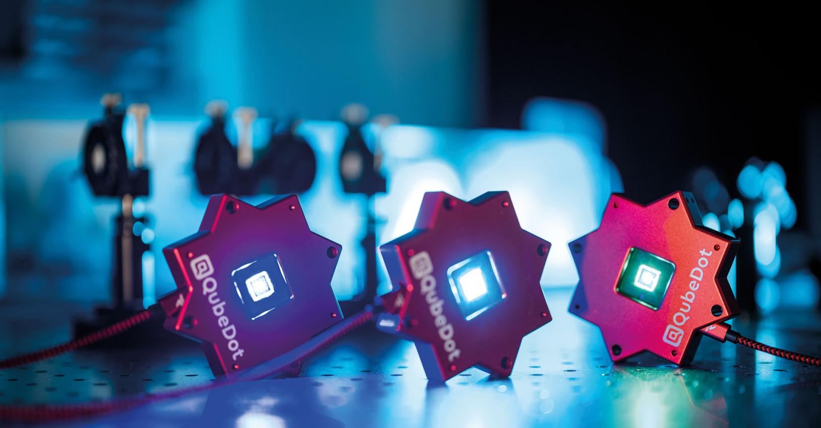
At QubeDot GmbH, a spin-off of the TU Braunschweig, we have asked ourselves these questions and, together with renowned research partners, have developed a platform technology as a solution. We call our technology SMILE – it’s short for Structured Micro-Illumination Light Engines.
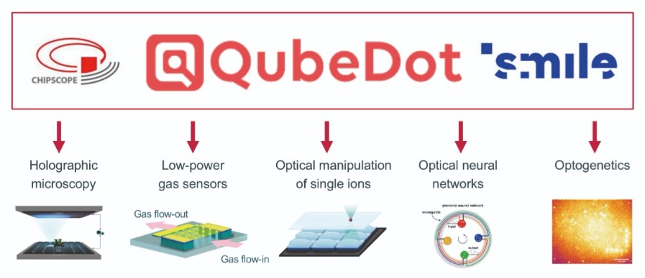
Figure 1. QubeDot and EU projects Chipscope and SMILE have led to versatile microLED platforms for different applications. More information is provided in the paper: H. S. Wasito et al. Beyond Solid State Lighting: Miniaturization, Hybrid Integration and Applications of GaN µLEDs, Applied Physics Reviews 2019
With these three steps, the technology is mature. However, it would still take significant effort on the customers’ side to use this to target applications. So, we help them by simplifying operability. It is easy to control the power of a laser with an analogue signal – but what if there are, for example, 256 light sources, all requiring a signal at the same time? To address this need we have written software that allows the user to immediately generate illumination patterns.
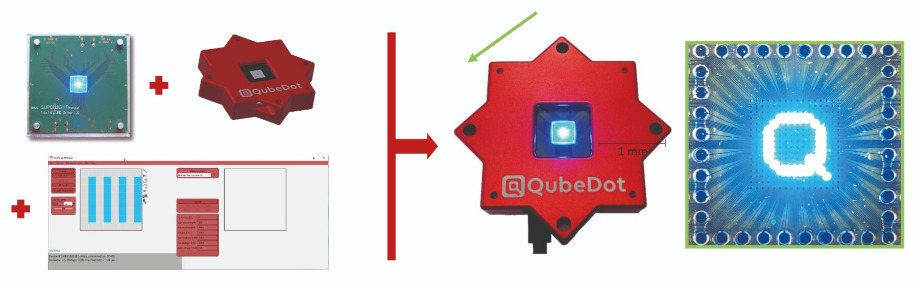
Figure 2. A SMILE platform consists of a microLED chip, electronics, housing and a Graphical User Interface (GUI).
SMILE specifications
The current SMILE platforms are formed as chip-on-board (COB) on common PCBs. With these options, early adopters have no difficulty in bringing microLED technology into their products and labs. Today, we offer two different versions of the SMILE platform: 8 by 8 pixels, and 16 by 16 pixels. All SMILE platforms always consist of the LED chip, the electronics, the housing and the control software (see Figure 2).
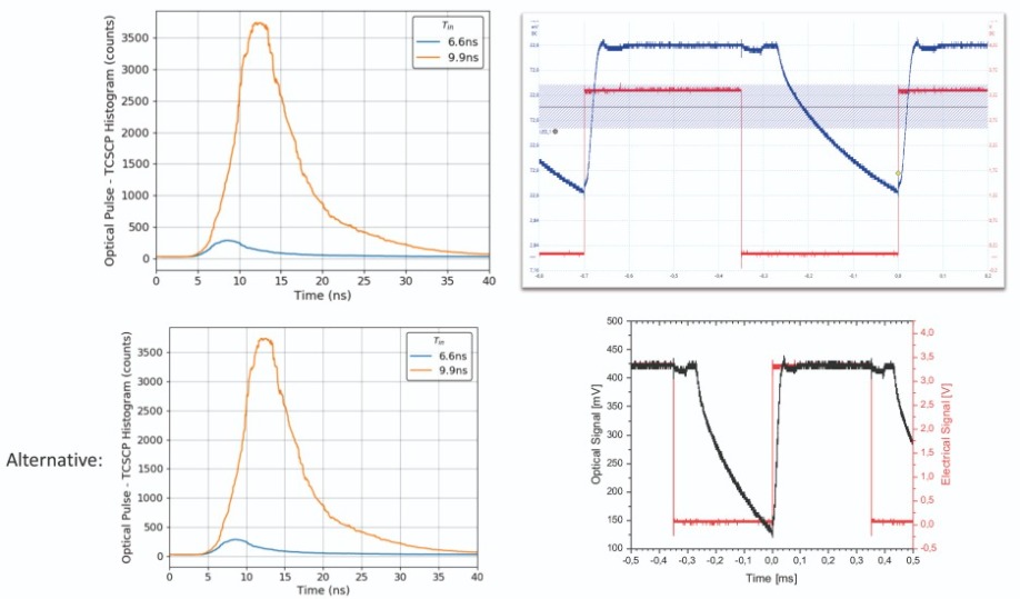
Figure 3. 100 MHz chip level modulation (left) and 3.330 MHz frame rate of a 16 by 16 SMILE platform (right) with the electrical stimulus in red and photodiode signal in blue.
When considering modulation speed capabilities, it’s important to distinguish between the chip level and the SMILE platform level. At the chip level we have evaluated modulation rates with time-correlated single-photon counting. This technique involves applying short electrical pulses to a microLED pixel and measuring its light output and its exact timing with a sensitive detector, such as a single-photon avalanche diode. Based on this approach, we have determined a modulation frequency for a 20 μm pixel in our 8 by 8 array of roughly 100 MHz, which corresponds to a pulse length of the order of 10 nanoseconds.
At the SMILE platform level, modulation is influenced by the surrounding electronics, and primarily its capacitances. For 16 by 16 SMILE platforms there are further limitations, associated with the synchronization of three microcontrollers. However, frame rates are still faster than those associated with the synchronization of multiple laser sources. For example, we have realised a rate of 3,333 frames per second, with the frame rate independent of image content (see Figure 3).
One of the questions we are asked most frequently at QubeDot is ‘What is your output power?’ The answer depends on the pixel’s size, its emission wavelength and the drive current. State-of-the-art epitaxy and chip processing ensure that output powers are as high as possible. We do not roughen the backside of the chip to enhance the light extraction efficiency because although this would increase the light coupled from the chip, the pixels would no longer be clearly delineated from one another in their optical appearance. That would be a significant downside, as it would result in a blurring of the luminous pattern from the roughened chip surface.
Here we illustrate the capability of our SMILE technology by showing the characteristics of an 8 by 8 platform that has a 75 μm pixel size, a 150 μm pitch and a 450 nm emission wavelength. The single optical output powers from the 64 individual LED pixels of this array operated at a range of voltages are shown in Figure 4. When controlling individual pixels, average output powers are around 384 μW at 3.3 V and 830 μW at 4.0 V. At the higher operating voltage, the optical power density is 14.7 W/cm². So, if all 64 pixels are switched on, this 8 by 8 SMILE platform will emit 15.2 mW at 4.0 V (and 6.7 mW at 3.3 V).
With this 8 by 8 SMILE platform, the user can precisely control and distribute the desired optical power in the projected image plane. This is accomplished because the spatial distribution of the emitting LEDs can be controlled independently from their individual output powers. Note that an additional knob for controlling the optical output power distribution and its grid density is the selection of the SMILE platform.
Another question that we are often asked is how small can we make our pixels. Since the GaN technology for manufacturing SMILE platforms is understood and mastered, we can routinely produce pixel sizes in the range of 5 ... 100 ... 500 μm. Pixel sizes below 5 μm work reliably in the lab and will be introduced to the market soon. Typically, initial customer tests always take place with a pixel size of 75 μm, as this evaluation allows us to determine the pixel size that should be employed. The pixels do not necessarily have to be square in shape – there are also applications where several microLED lines are required. As one can imagine, there are countless combinations of size, pitch, wavelength, lighting pattern, LED output power control and modulation control for targeting a thousand-and-one different applications.
Optimising optogenetics
One group using our SMILE platform is led by Maria Leilani Torres and Alexander Heisterkamp from the Institute of Quantum Optics in Leibniz University Hannover, Germany. In the Optogenetics lab at NIFE, Hannover, their team employs fluorescence imaging, captured at a high frame rate, to visualize calcium fluctuations in cells, using a calcium-sensitive dye and a CMOS-camera. The calcium dye has been selected in combination with an orange LED that emits at 590 nm, to ensure that excitation does not affect the activity of the rhodopsin channel. Using the SMILE platform, cell cultures are stimulated by different illumination patterns. A series of images, shown in Figure 5, illustrates how nine microLEDs can trigger a wave of electrical activity.
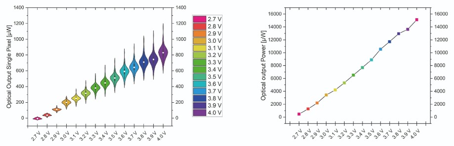
Figure 4. 75 µm pixel size 8 by 8 SMILE platform emitting at 450 nm. Violin graph of individual pixel output powers at different bias voltages (left) and overall output powers if all pixels are switched on (right). Measurements were conducted with a 10-inch integrating sphere.
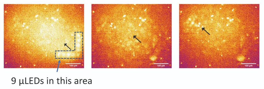
Figure 5. Nine microLEDs in the lower right trigger a wave of electrical activity from this lower right corner to the upper left corner. The arrows indicate the flow of calcium, visualized by the fluorescent calcium sensitive dye.
Opportunities ahead
We have no doubt that our SMILE technology will find deployment in various applications. Its use in optogenetics, highlighted here, is just one of many possibilities. One of its great strengths is that it can be used directly ‘out of the box’ – the same cannot be said for systems based on lasers. The form of SMILE presented here, known as red star, is not suitable for all users. But given our mastery of microLEDs, and our expertise with the SMILE platform, we can easily tailor this technology for our customers. This solution is available now, and can start with small quantities, an unusual but welcome aspect for early adopters.
The SMILE project has received funding from the European Union’s Horizon 2020 research and innovation programme under grant agreement No 952135. More information can be found via qubedot.com and smile-technology.eu


