
Point defects: the ultimate blue LED efficiency killers

A previously unknown class of intrinsic light-quenching point defect is unveiled in InGaN quantum wells
BY THOMAS WEATHERLEY, CAMILLE HALLER, YAO CHEN, JEAN-FRANÇOIS CARLIN, RAPHAËL BUTTÉ AND NICOLAS GRANDJEAN FROM EPFL
TODAY’S InGaN-based LEDs are enjoying tremendous success in general and automotive solid-state lighting. However, this is by no means the limit of their reach – intense industrial and academic research is driving efforts to shrink the dimensions of this device below 10 μm, a feat that will enable the production of microLED displays for augmented/virtual reality, wearable devices, and smartphones.
Deployment of LEDs in all these applications is dependent on the remarkable conversion efficiency of injected electron-hole pairs into photons within the InGaN/GaN quantum wells that lie at the heart of these devices. This light-generating internal quantum efficiency can exceed 90 percent for blue LEDs, even when the threading dislocation density in the epilayer is as high as 108 cm-2. Yet there is a rarely-discussed feature of these LEDs which is crucial to this impressive performance: the ‘underlayer’.
Commercial blue/near-UV LEDs are exclusively grown by MOCVD, and their structure always contains an underlayer – either a thick, low-indium-content InGaN layer, or an InGaN/GaN superlattice (see Figure 1 (a)). The motivation for including this underlayer, which sits beneath the quantum wells, is highlighted in device measurements that underscore the hike in efficiency it provides (see Figure 1 (b)).
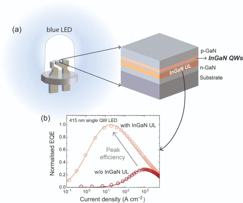
Figure 1: (a) Blue LEDs have an active region containing InGaN/GaN quantum wells (QWs). All commercial structures also include a low indium content underlayer (UL, in brown). (b) External quantum efficiency (EQE) related to current density for two blue-emitting LED structures, with and without an underlayer. Using the underlayer brings a near four-fold increase in peak efficiency.
Working at EPFL, our team carefully considered all of these explanations, before ruling them out, one by one (see Further Reading). Through careful research, we can now uncover the real reason behind the benefit of the underlayer: it counteracts point defects which act as nonradiative recombination centres inside the InGaN wells.
These previously unknown point defects have a strong interaction with indium, so the introduction of an InGaN underlayer provides a sink to trap them before they can reach the quantum well. Failure to use this underlayer allows the point defect density inside the wells to reach as high as 1016 cm-3, killing the quantum efficiency of blue-emitting LEDs.
Elucidating the role of the underlayer
In our proposed mechanism, we hypothesise that when there is no underlayer, point defects are present in the InGaN quantum wells. Adding an underlayer traps these defects, leaving a high-efficiency quantum well (see Figure 2).
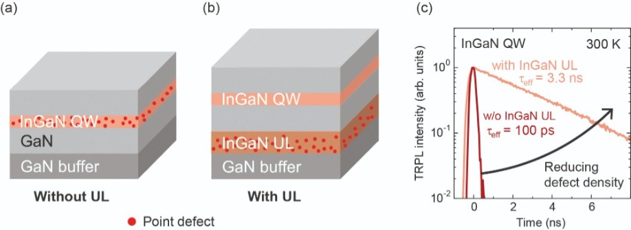
Figure 2: (a) and (b) show proposed scenarios for growth without and with an underlayer (UL), respectively. Without an underlayer, there is a high concentration of point defects in the quantum well, whereas using an underlayer traps the point defects before the quantum well. (c) Examples of time-resolved photoluminescence (TRPL) decay curves obtained on samples with and without an underlayer; the increase in quantum well-effective carrier lifetime (related to the slope of the decay) with the addition of an underlayer clearly indicates a reduction in the point defect density in the quantum well.
As all other parameters are unchanged between samples, any increase in the effective carrier lifetime is attributed to a decrease in the nonradiative recombination rate and hence a lower point defect density inside the well (see Further Reading for more details). Unsurprisingly, the underlayer provides a huge increase in the quantum-well effective carrier lifetime (see Figure 2 (c)), a trait indicative of a drastic decrease in the point defect density inside the well. This begs the question: what is the key ingredient in this underlayer that excels in trapping point defects?
To try and answer this, we grew a series of samples in an Aixtron 3 x 2-inch showerhead MOCVD reactor, making changes to underlayer materials and thicknesses. We used 2-inch Sumitomo Electric freestanding GaN substrates with a dislocation density of only about 106 cm-2 (see Figure 3 (a)).
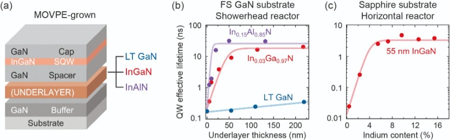
Figure 3: (a) The standard structure used by the researchers at EPFL is a 2.7 nm-thick In0.12Ga0.88N single quantum well. The underlayer material is varied in this structure between GaN grown at low-temperature (LT), InGaN, and InAlN. (b) Quantum-well effective carrier lifetime against the underlayer thickness for these three materials for samples grown in a showerhead MOCVD reactor on freestanding (FS) GaN substrates. The more indium an underlayer contains, the more immediate the effective carrier lifetime improvement is, indicating a more rapid decline in the point defect density. Using just GaN results in barely any improvement. The critical role that indium plays in the underlayer is emphasised in (c), which demonstrates that a similar point defect density reduction can be obtained without changing the underlayer thickness, but by simply increasing the indium content in the InGaN alloy; this sample series was grown in a horizontal reactor on sapphire substrates. Lines indicate fits to the experimental data obtained using a surface defect burying model.
Far better results are realised by introducing indium to the underlayer. The addition of an indium content of just 3 percent yields a dramatic improvement in the effective carrier lifetime, even for an underlayer thickness of just 50 nm. This benefit, stemming from a massive decrease in the point defect density in the well, underlines the importance of indium to the defect-trapping process.
To illustrate the role of indium, we grew another series of samples with underlayers of identical thickness but varying indium content (see Figure 3 (c)). Measurements on these samples show that increasing the indium content has the same effect in reducing point defects as increasing the underlayer thickness. This result demonstrates that it is the sheer quantity of incorporated indium atoms that governs the number of trapped point defects.
Notably, this indium-content sample series was grown using a different MOCVD reactor – an Aixtron horizontal 200/4 RF-S – and on sapphire substrates, confirming that the indium-related point defect trapping mechanism is independent of precise substrate or reactor conditions. More recent work has demonstrated that even for samples grown on silicon (111) substrates, which can have dislocation densities as high as 1010 cm-2, trapping point defects using an underlayer is still crucial to attain high-efficiency InGaN quantum wells.
Since indium plays the critical role in this mechanism, there is no reason to be restricted to using InGaN underlayers. In its place could be an InAlN underlayer that’s nearly lattice-matched to GaN, allowing the same defect density reduction. We tested this hypothesis, finding that InAlN is an attractive alternative (see Figure 3). With InAlN, there is a larger indium content in the underlayer, typically 15 percent. Consequently, it is possible to realise the same point-defect-density reduction, and hence efficiency improvement, with a thinner underlayer.
Drawing on these results, we propose a specific chronology. Initially, there are surface defects present during GaN buffer growth. During subsequent GaN growth, these defects remain at the surface, until the growth of any indium-containing layer. When indium is introduced, these atoms interact with surface defects to form nonradiative point defects in the bulk material.
Using this concept, we developed a model that links the key properties of the underlayer, such as its indium content and its thickness, to the effective carrier lifetime in the InGaN quantum well. Fitting the data with this model, where crucially the term defining the interaction efficiency of the surface defects with the indium atoms is the same across all sample series (see Further Reading), confirms that indium alone plays the critical role in incorporating these surface defects to form point defects (see Figure 3).
Following on from this finding, we pinned down the origin of these surface defects. Since they seem to arise from the GaN buffer, we considered the impact of any difference in the growth conditions of this layer to that of the rest of the structure. For many III-nitride heterostructures, to ensure a flat surface morphology, it is common practice to grow the GaN buffer at very high temperatures (around 1000 °C): we wondered whether this higher temperature is behind the generation of surface defects.
To determine whether this is the case, we grew another portfolio of samples. No underlayer was included in this series; instead, we varied the growth temperature of the GaN buffer and monitored the effect on the quantum well (see Figure 4 (a)). We found that raising the growth-temperature of the buffer directly reduced the effective carrier lifetime in the quantum well (see Figure 4 (b)). Based on this observation, we can conclude that surface defects are generated by high-temperature GaN growth, with temperatures of around 850 °C or more threatening to drag down quantum-well efficiency.
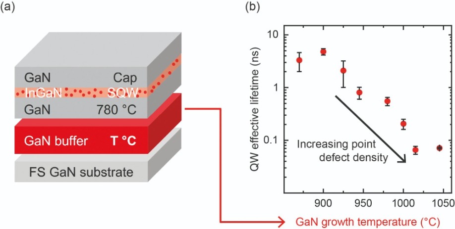
Figure 4: (a) EPFL’s new sample series structure, containing no underlayer. Instead, the growth temperature, T, of the GaN buffer beneath the In0.12Ga0.88N single quantum well is varied to test whether surface defect creation is related to high-temperature growth. (b) The drastic decrease in quantum-well effective-carrier-lifetime on increasing the growth temperature for the GaN buffer demonstrates that high-temperature GaN growth is directly responsible for generating surface defects, which then interact with indium in the quantum well to form nonradiative recombination centres.
Our final view is that the formation of the efficiency-sapping point defects in the quantum wells begins with the generation of surface nitrogen vacancies, formed during high-temperature GaN growth. These vacancies remain at the surface during the growth of any low-temperature GaN layers that follow. When an indium-containing layer is grown – this could be the underlayer, or a quantum well – nitrogen vacancies interact with indium atoms to form point defects in the bulk that act as nonradiative recombination centres. At this stage it is critical to recognise that the nature of these final nonradiative recombination centres buried in InGaN is still unknown. They may take the form of group-III-nitrogen divacancies, or even a group-III vacancy associated with an impurity such as oxygen.
Imaging point defects
The work we have discussed so far has enabled us to fully elucidate the roles of both the underlayer and point defects on the quantum efficiency of InGaN/GaN quantum wells. To get this far, it was essential to exclude previous explanations that are non-defect related, a task we accomplished by producing many different carefully designed sample series. Such work requires much thought and consideration, partly because the effective carrier lifetime is an indirect metric for point defect density, and is sensitive to a variety of factors that include well structure, disorder, electric field, and strain. Clearly, our findings would be more compelling if we had a direct estimation of the actual point defect density in the well. To do this, we need a way to directly detect and even image the point defects that are buried inside the quantum well.
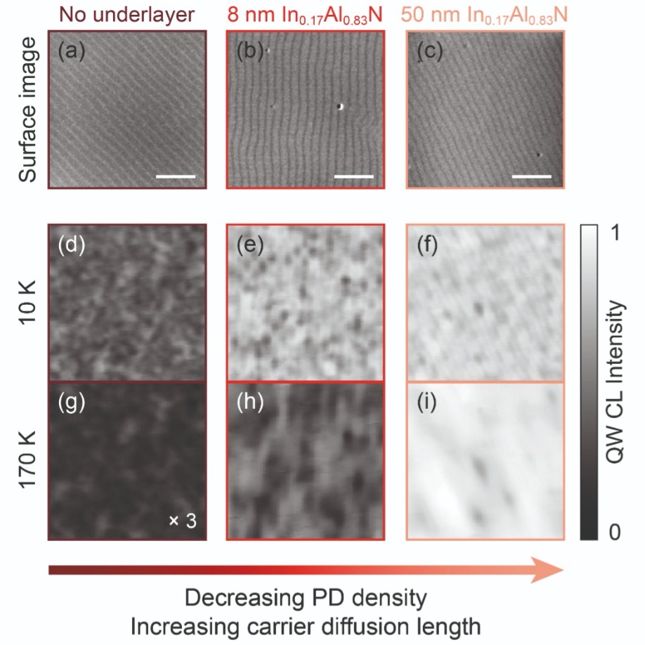
Figure 5: (a–c) Secondary electron images for three In0.15Ga0.85N/GaN single-quantum-well samples with different thickness In0.17Al0.83N underlayers; these images show the surface morphology of the samples. Step-edges are clear as parallel lines and V-shaped pits marking the position of threading dislocations are visible as dark spots. All are 2 µm x 2 µm (500 nm scale bar). (d–f) show the quantum-well cathodoluminescence (CL) intensity images of the same 2 µm x 2 µm area for each sample at 10 K. Dark regions have no correlation with dislocation positions, and are instead a direct consequence of non-radiative recombination at single point defects. The decrease in density of the dark spots as the underlayer thickness is increased represents a decrease in point defect density. As the temperature is raised to 170 K, CL images on the same area again (g–i) clearly illustrate that nonradiative recombination is thermally activated. The loss of resolution in these 170 K images also indicates an increase in carrier diffusion length. Each image is plotted on an absolute intensity scale from 0 – 1. The 170 K intensity for the sample without an underlayer has been multiplied by three to make the image visible.
To overcome these issues, we turned to cathodoluminescence. Using this technique, we scanned an electron beam over the quantum well at scales below the diffraction-limit of light. By collecting luminescence intensity from the sample at each electron-beam excitation position, we built up a cathodoluminescence intensity map of the scanned area. Defects present in this area appear as dark regions in the image, due to local nonradiative recombination of excited carriers.
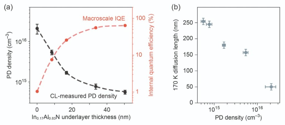
Figure 6: (a) Point defect (PD) densities inside the InGaN/GaN quantum well as the InAlN underlayer thickness is varied, measured directly from similar cathodoluminescence (CL) images to those in Figure 5. These densities are compared to the macroscale internal quantum efficiency (IQE) measured for the same samples using time-resolved photoluminescence at room temperature. As expected, the drop in point defect density is directly reflected by a huge rise in IQE. Carrier diffusion lengths are also measured by CL at 170 K, and are compared to the PD densities in (b). Decreasing the PD density to less than 1015 cm-3 (thickest underlayer sample) leads to a significant increase in the carrier diffusion length. Dashed lines are guides to the eye.
Cathodoluminescence images obtained from 2 μm by 2 μm scans of the quantum-well samples are shown in Figure 5. In images obtained at 10 K, dark spots that are unrelated to dislocations are immediately clear. Each of these spots corresponds to a single killer nonradiative point defect inside the well. From this experiment it is easy to directly see the impact of the underlayer: the number of dark spots drastically decreases as the underlayer thickness increases, because this drives down the point defect density in the quantum well.
Differences between the samples are more obvious when measurements are made at 170 K (see Figure 5 (g) to (i)). Due to the thermally-activated nature of defect-related nonradiative recombination, at this temperature each point defect has a much greater impact on the cathodoluminescence intensity. The increased thermal energy also leads to longer carrier diffusion lengths and hence a reduction in the spatial resolution, visible as a smoothening of the images compared with those obtained at 10 K. Note that the less-defective samples have much smoother cathodoluminescence images at 170 K (see Figure 5(i)) than the highly-defective samples (see Figure 5(g)); this directly indicates an increase in carrier diffusion length as the point defect density in the quantum well reduces.
Careful analysis of these cathodoluminescence images (see Further Reading) has enabled us to extract point defect densities and 170 K carrier diffusion lengths for five samples with different underlayer thicknesses (see Figure 6). Comparing these properties to the macroscale room-temperature internal quantum efficiencies measured by time-resolved photoluminescence provides a clear, unequivocal picture of the roles of the underlayer and of point defects: inserting an underlayer decreases the point defect density in the well from 1016 cm-3 to around 1014 cm-3, enabling macroscale efficiency at room temperature to rise from only 1 percent to above 60 percent. Another insight is that adding a thick underlayer leads to a significant increase in the carrier diffusion length. Based on these findings, taking these killer point defects into account is crucial when designing microLEDs.
The road ahead
There is merit in revisiting previous design decisions, armed with this new knowledge of indium-interacting point defects and the underlayer mechanism in InGaN/GaN quantum well structures. For instance, we can now see that the low indium content cladding layers in InGaN-waveguide laser diodes are probably behaving as underlayers, improving device efficiency. But several questions remain: is one of the reasons behind the success of multiple-quantum-well structures that the lower quantum wells act as underlayers, ensuring high-quality upper quantum wells? How many previous results were skewed, due to unaccounted point defects inside the well? Is growing GaN at high temperatures, on balance, detrimental or beneficial? Could these point defects be related to the ‘green gap’, the phenomenon behind the low efficiency of high-indium-content InGaN quantum wells? The implications of our findings are widespread, and they require much further investigation.
Note, though, that having unlocked direct imaging of nonradiative point defects inside heterostructures, we can now more easily detect intrinsic point defects. In addition to visible LEDs, these defects might be limiting the performance of other III-nitride devices, such as deep-UV LEDs. Our advances in imaging are also laying the foundation for new point defect studies, including time-resolved measurements at a single buried point defect.
Further Reading
C. Haller et al. Burying non-radiative defects in InGaN underlayer to increase InGaN/GaN quantum well efficiency. Appl. Phys. Lett. 111 262101 (2017)
C. Haller et al. GaN surface as the source of non-radiative defects in InGaN/GaN quantum wells. Appl. Phys. Lett. 113 111106 (2018)
Y. Chen et al. GaN buffer growth temperature and efficiency of InGaN/GaN quantum wells : The critical role of nitrogen vacancies at the GaN surface. Appl. Phys. Lett. 118 111102 (2021)
T. F. K. Weatherley et al. Imaging nonradiative point defects buried in quantum wells using cathodoluminescence. Nano Lett. 21 5217-5224 (2021)


