
Glasgow team finds novel way to print zinc oxide nanowires
A new method of ‘sliding’ delicate high-performance electronics onto flexible surfaces could enable future developments in electronics, scientists say.
Engineers from the University of Glasgow claim they have found a way to solve one of the key problems of contact printing – a method of planting electronics onto bendable plastic surfaces to create flexible electronic circuits and devices.
The ability to reliably reproduce the same device at high volumes is key to developing an electronic product and bringing it to market. While contact printing techniques have been in development for more than a decade, scientists have struggled to create reliable methods of bringing together their electronic elements and surfaces over and over while keeping the prints precisely aligned and at the required uniformity.
Now, in a new paper ‘Development of a highly controlled system for large-area, directional printing of quasi-1D nanomaterials’ published in the journal Microsystems & Nanoengineering, researchers from University’s Bendable Electronics and Sensing Technologies (BEST) describe how introducing a sliding motion to the contact printing technique has helped them apply nanowires to both bendable and rigid surfaces with greater accuracy.
The team began by fabricating zinc oxide nanowires, similar to those already used in many high-performance sensor designs, on a rigid surface in the lab.
They designed an automated system to transfer the nanowires from their surface they were created on – the ‘donor’ surface – to a sheet of flexible silicon – the ‘receiver’ surface.
The system allows the team to mechanically control the movements of two flat platforms, which can pivot to ensure they align correctly to make the transfer happen smoothly. The motion of the platforms is similar to the palms of two hands meeting and sliding away from each other, with a flat object clasped in one palm passing to the other in the process.
The donor and receiver surfaces are placed between the two platforms, which come together with carefully controlled alignment. The system allows the team to maintain precise control over the lateral and shear forces on the surfaces when they meet and when they slide apart, which is key to allowing the nanowire to transfer cleanly to the flexible surface.
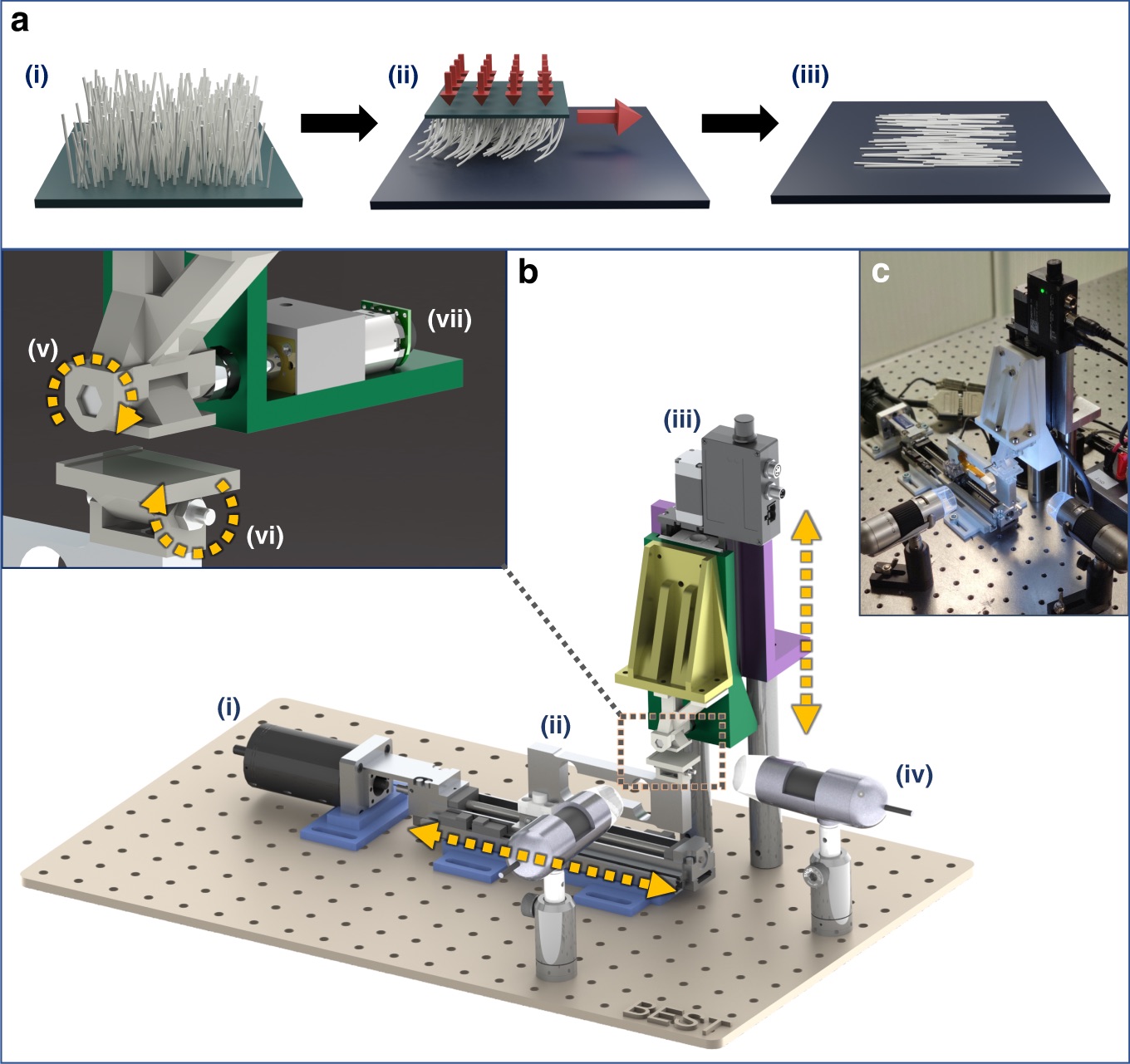
The picure above shows these stages: a Steps of the contact printing process: i donor substrate with vertically grown nanowires; ii sliding of the donor substrate across the receiver substrate, while also applying pressure; iii printed nanowires on the receiver substrate aligned along the direction of sliding. b 3D model of the designed contact printing system: i horizontal actuator; ii load cell; iii vertical actuator; iv microscopes for alignment monitoring; v self-aligning donor substrate platform (primary axis); vi self-aligning receiver substrate platform (secondary axis); and vii mechanism for fixing the tilt of the platform. c Image of the assembled system
They showed a high level of uniformity of alignment of the nanowires on the surfaces, suggesting that the new process could be a useful next step towards mass-scale contact printing of nanowires on flexible surfaces.
Ravinder Dahiya of the University of Glasgow’s James Watt School of Engineering leads the BEST group.
Dahiya said: “This is a simple but effective technique which we think has a lot of potential to address one of the key problems of contact printing to date.
“The paper discusses the ability of the system to print reliably on a relatively small area, only because we were limited by the size of the printing apparatus we built. There is every reason to expect that the same process could work over much greater surface areas, allowing the creation of large-scale flexible electronics with a level of reproducibility that has been very difficult to achieve before now.
“Although the paper demonstrates the technique using zinc oxide nanowires, the method could be used to create printed integrated circuits using materials like silicon and. The new system could also support layer-by-layer printing, allowing the development of vertically-integrated circuits.
“In parallel with this research, we have also developed a new way to reliably transfer the semiconductors onto flexible surfaces. Combining our direct roll printing and the new sliding processes to printed semiconductor micro and nanowires could open up many new applications for high-performance flexible electronics.
“That could include adding a sophisticated sense of ‘touch’ to prosthetics, or developing advanced wearable devices for keeping precise track of hospital patients’ vital signs, or finding new forms of self-contained, fully bendable digital displays.”
The research was supported by funding from the Engineering and Physical Sciences Research Council (EPSRC).


