
Guiding Excitons in 2D Materials
Researchers create 'excitonic' wires that could enable 2D compound semiconductor devices based on straintronics
Physicists at City College of New York and their collaborators in Japan and Germany have announced an advancement in the study of excitons (electrically neutral quasiparticles that exist in insulators, semiconductors and some liquids).
They have created an 'excitonic' wire, or one-dimensional channel for excitons. They hope this in turn could result in innovative devices that could replace certain tasks that are now performed by standard transistor technology.
Florian Dirnberger, post-doc in Vinod Menon’s research group in CCNY’s Center for Discovery and Innovation, and one of the lead authors of the study that appears in the journal Science Advances, detailed the team’s breakthrough. “Our main achievement was to manage to create these excitonic wires, essentially one-dimensional channels for excitons, in what is otherwise a two-dimensional semiconductor,” he said.
“Since charge neutral excitons are not simply controlled by external voltages, we had to rely on a different approach. By depositing the atomically thin 2D crystal on top of a microscopically small wire, a thousand times thinner than a human hair, we created a small, elongated dent in the two-dimensional material, slightly pulling apart the atoms in the two-dimensional crystal and inducing strain in the material. For excitons, this dent is much like a pipe for water and once trapped inside, they are bound to move along the pipe, realising quasi one-dimensional transport of excitons.”
To do this, they built a hybrid 1D/2D structure. The active component that hosts the excitons is a monolayer (1L) WSe2, fully encapsulated in high-quality hexagonal BN (hBN) to provide uniform dielectric screening and suppress disorder. The hBN-WSe2 stack is then placed on top of a GaAs/Al0.36Ga0.64As core/shell nanowire and is deformed to a 90-nm height over a length of about 8 μm.
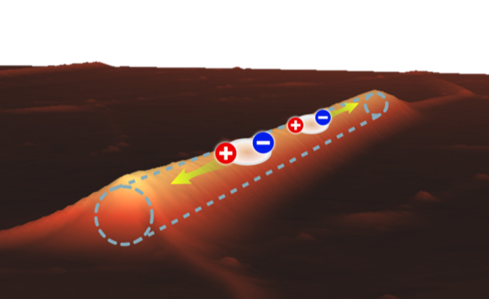
The picture above shows the topography of the 2D crystal on top of the microscopically small wire indicated by dashed lines. Excitons freely move along the wire-induced dent, but cannot escape it in the perpendicular direction.
Possible outcomes include innovative devices based on excitons that operate at room temperature and could replace certain tasks performed by contemporary transistor technology.
In addition to Dirnberger and other members of Menon’s lab at CCNY, researchers led by Alexey Chernikov at Dresden University of Technology, and at the University of Regensburg (both Germany) participated in the study, along with researchers from Japan’s National Institute for Materials Science.
'Quasi-1D exciton channels in strain-engineered 2D materials' by Florian Dirnberger et al; Science Advances 29 Oct 2021 Vol 7, Issue 44


