
Korean team Makes perovskite breakthrough
New research reveals the easy tunability of SrTiO3 perovskite material, opening doors to its widespread use in next generation electronics
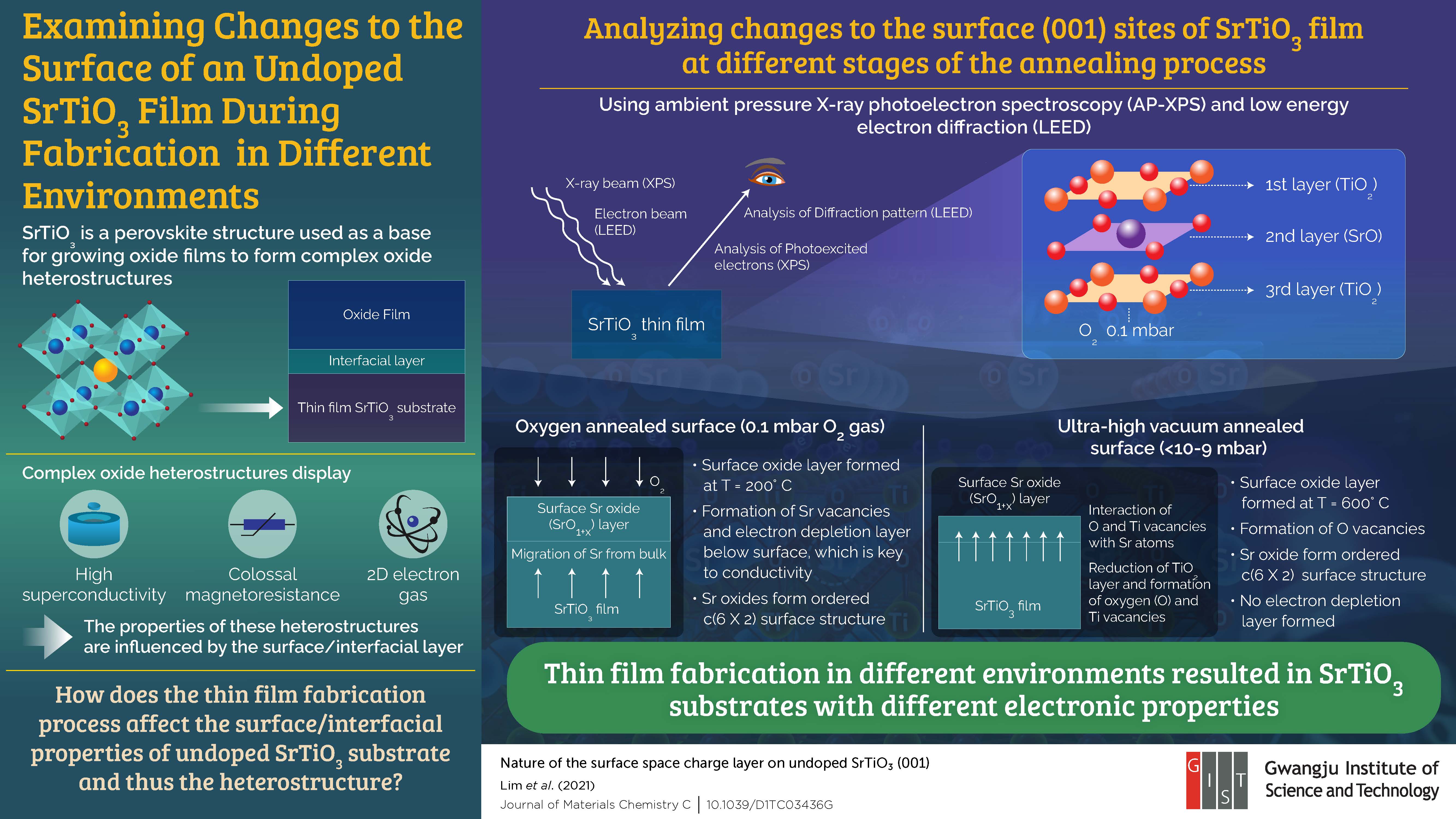
In a new study, researchers from Korea highlight how fabrication of thin films of a particular perovskite in different environments leads to altered electronic properties. This flexibility allows for the development of films with tunable electronic properties, opening doors to a wide variety of next generation electronic devices.
Perovskites' cubic-like crystal lattice makes them suitable for use as a base for growing oxide films to form heterostructures with unique electrical properties. The properties of these heterostructures depend on the charge transfer in the interfacial layer between the perovskite substrate and oxide overlayer. This charge transfer can be manipulated via either doping or through the fabrication process.
The Korean team led by Bongjin Simon Mun from Gwangju Institute of Science and Technology, use ambient pressure X-ray photoelectron spectroscopy (AP-XPS) and low energy electron diffraction (LEED) to investigate how fabrication conditions (annealing in an oxygen-rich environment and an oxygen deficit, low-pressure environment) for a particular perovskite material, SrTiO3—one of the most popular substrates for growing oxide films—affects its undoped surface and the resulting interfacial layer of the heterostructure. By using an undoped surface, the researchers wanted to examine the changes that occur on the surface of the substrate without interference from the dopants. “The presence of doping can interfere with correct interpretation of the surface defect states, which can be critical to apprehend the electrical properties of heterostructures. Our study on undoped SrTiO3 provides unbiased characteristics of SrTiO3 substrate,” says Mun. Their findings were made available online on 16 September 2021 and published in Volume 9 Issue 38 of the Journal of Materials Chemistry C.
In the oxygen environment, an electron depletion layer formed as the Sr atoms in the substrate migrated to the surface of the film to react with oxygen and form a stable oxide layer. In the low-pressure oxygen deficit environment, the formation of such a depletion layer was limited as the oxide layer was formed due to the reduction of the TiO2 layer that generated electrons.
In both environments, a similar oxide layer was formed, but the electronic properties of the structure differed as the electron depletion layer is key to the conductivity of the structure. “Our work shows clearly how the electrical properties of devices can be tuned by adjusting the population of electrons near the surface region, which is a very fundamental and important result indicating that future electronic devices can be realized with material characterization at the atomic level,” says Mun. “In the long run, our study on SrTiO3 will lay out a solid foundation for advanced electronic devices that will enable a better lifestyle for us.”
'Nature of the surface space charge layer on undoped SrTiO3 (001)' by Hojoon Lim et al; Journal of Materials Chemistry C 2021


