Loading...
News Article

Navitas Opens World's First EV GaN chip Design centre

News

Company will work in partnership with OBC, DC-DC and traction system companies

Navitas Semiconductor has announced the opening of a new electric vehicle (EV) design centre, further expanding into higher-power GaN markets.

The design centre, based in Shanghai, China, hosts a team of power system designers with capabilities across electrical, thermal and mechanical design, software development, and complete simulation and prototyping capabilities. EV customers will be supported worldwide by the new team, from concept to prototype, through to full qualification and mass production.

Industry-expert, Hao Sun, the new senior director of the Shanghai design centre, said: "The design centre will develop schematics, layouts, and firmware for full-function, productisable EV power systems. Navitas will work in partnership with OBC, DC-DC and traction system companies to create innovative, world-class solutions with the highest power density and highest efficiency to propel GaN into mainstream eMobility."

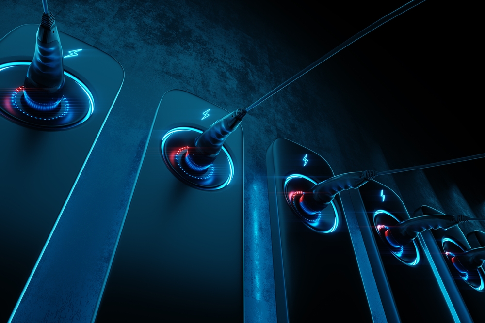
High-power 650V GaN ICs tailored to EV applications were sampled to EV customers in December. A 6.6kW OBC concept was displayed at the recent Xiaomi Portfolio Demo Day, and is shown at CES '22.

"The Navitas EV team has rich talent and proven experience delivering power systems," said Charles Zha, VP and GM of Navitas China. "EMobility is an exciting expansion market for GaN, with an estimated $250 potential content per EV. Market-by-market, Navitas is making swift progress into higher-power applications, like EV, data centre and solar."

SiC MOSFETs: Understanding the benefits of plasma nitridation
Wolfspeed reports Q2 results
VueReal secures $40.5m to scale MicroSolid printing
Mitsubishi joins Horizon Europe's FLAGCHIP project
Vishay launches new high voltage SiC diodes
UK team leads diamond-FET breakthrough
GaN adoption at tipping point, says Infineon
BluGlass files tuneable GaN laser patents
QD company Quantum Science expands into new facility
Innoscience files lawsuit against Infineon
Riber revenues up 5% to €41.2m
Forvia Hella to use CoolSiC for next generation charging
Photon Design to exhibit QD simulation tool
Ortel transfers CW laser fabrication to Canada
Luminus adds red and blue multi-mode Lasers
PseudolithIC raises $6M for heterogeneous chiplet tech
Mesa sidewall design improves HV DUV LEDs
IQE revenue to exceed expectations
'Game-changing' VCSEL system targets clinical imaging
German start-up secures finance for SiC processing tech
Macom signs preliminaries for CHIPS Act funding
IQE and Quintessent partner on QD lasers for AI
EU funds perovskite tandems for fuel-free space propulsion
EU to invest €3m in GeSi quantum project
Transforming the current density of AlN Schottky barrier diodes
Turbocharging the GaN MOSFET with a HfOâ‚‚ gate
Wolfspeed launches Gen 4 SiC MOSFET technology
Report predicts high growth for UK's North East
Element Six unveils Cu-diamond composite
SemiQ launches hi-rel 1700V SiC MOSFETs
Lynred to exhibit Eyesential SWIR sensor for machine vision
Thorlabs buys VCSEL firm Praevium Research
×
Search the news archive

To close this popup you can press escape or click the close icon.
Logo
x
Logo
×
Register - Step 1

You may choose to subscribe to the Compound Semiconductor Magazine, the Compound Semiconductor Newsletter, or both. You may also request additional information if required, before submitting your application.


Please subscribe me to:


You chose the industry type of "Other"

Please enter the industry that you work in: