
Scientists weave nanoribbons from nanowires
Mass-producing nanoribbons for cutting-edge electronics and catalysts
Researchers from Tokyo Metropolitan University have succeeded in using nanowires of a transition-metal chalcogenide to make atomically thin “nanoribbons”.
Bundles of nanowires were exposed to a gas of chalcogen atoms and heat which helped merge the threads into narrow strips. Given the scalability of the method, the team hopes it could see widespread use in industrial production.
As circuitry get smaller, faster, and more energy efficient, scientists are faced with the challenge of controlling the atomic-level structure of the materials that are used in them. One promising avenue of research is the use of intricate threads of material only a few atoms wide; one such structure is composed of transition-metal chalcogenides.
Atomically thin “nanowires” possess properties unique to their one-dimensional structure. But what they have in minuteness, they lack in tunability. This is where “nanoribbons” come in, that is, narrow, atomically thin sheets. Fine control of their width, for example, leads to controlled variation in their electronic and magnetic properties.
A great deal of work has been applied to “build” nanoribbons from the bottom up. The problem, however, is that such methods aren’t very scalable.
Now, a team led by Hong En Lim and Yasumitsu Miyata from Tokyo Metropolitan University have come up with a scalable way of assembling nanowires into nanoribbons.
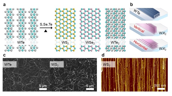
By taking tungsten telluride nanowires, they created bundles of wires deposited on a flat substrate. These were exposed to vapours of different chalcogens like sulphur, selenium and tellurium. With a combination of heat and vapour, the initially separate threads in the bundles were successfully woven together into narrow, atomically thin “nanoribbons” with a characteristic zigzag structure.
By tuning the thickness of the original bundles, they could even choose whether these ribbons were oriented parallel to the substrate or perpendicular to it, thanks to a competition between how favourable it is to have edges or faces parallel to the bottom surface. Furthermore, by tuning the substrate on which the bundles are placed, they could control whether the ribbons were randomly oriented or pointing in a single direction.
Importantly, the method is scalable and may be applied to take the synthesis from lab-scale manufacture of a few ribbons to bulk syntheses over large substrate areas.
The team were able to confirm that the ribbons they created had the exotic electronic properties which are unique to their one-dimensional nature.
The picture above shows: (a) Bundles of tungsten telluride nanowires are exposed to a chalcogen vapour and heated, converting the bundles into narrow, atomically thin strips of transition-metal chalcogenide. (b) Bundles of nanowire may be converted into ribbons oriented both vertically and horizontally with respect to the substrate. (c) Randomly and (d) unidirectionally oriented nanoribbons may be made using different substrate material.
REF
'Nanowire-to-Nanoribbon Conversion in Transition-Metal Chalcogenides: Implications for One-Dimensional Electronics and Optoelectronics' by Hong En Lim et al; ACS Appl. Nano Mater. 2021


