
Producing normally-off RF HEMTs
Plasma treatment and wet etching yields RF GaN HEMTs
A team from National Yang Ming Chiao University, Taiwan, claims to have produced the first normally-off GaN HEMTs using a digital etching technique.
According to spokesman for the team, Ping-Yu Tsai, RF devices benefit from normally-off operation because they can then be driven with just a single positive voltage. “This can reduce the complexity of IC design and save power consumption of the system modules, since the device does not consume energy when it is not operating,” added Tsai.
There are several reports of using a digital etch to recess the gate of power HEMTs, which have larger dimensions. Tsia and co-workers believe that they are breaking new ground by being the first team to apply this technique to RF HEMTs.
“We used this method to control the gate recess for RF HEMTs with a small gate length,” explained Tsai. By providing good control of the etch depth, the team demonstrated E-mode devices and RF characteristics.
Realising high-quality gate etching is not easy, demanding precise control of the etching depth while ensuring a low surface damage and good uniformity. Gate etching tends to involve the use of a plasma formed from either chlorine gas or BCl3, but both options promote damage on the surface of the gate, and ultimately impair the device’s performance and reliability.
To improve gate etching quality, Tsai and co-workers turned to a two-step digital etch. To optimise that approach prior to device production, they began by studying the impact of surface chemistry and etch rate on an AlGaN/GaN heterostructure comprising a buffer layer, an un-doped GaN channel, a 1 nm-thick AlN spacer and a 22 nm-thick Al0.22Ga0.78N barrier layer.
After adding a SiN hard mask to this heterostructure and patterning it by photolithography and fluorine-based inductively coupled plasma etching, the team oxidized the wafer with two different techniques: exposure to hydrogen peroxide for 5 minutes; and oxidation of the wafer in an oxygen plasma, using an inductively coupled plasma system operating at a range of RF powers. Both approaches were followed with an identical second step: a 90 s digital etch in diluted HCl to remove the oxide products.
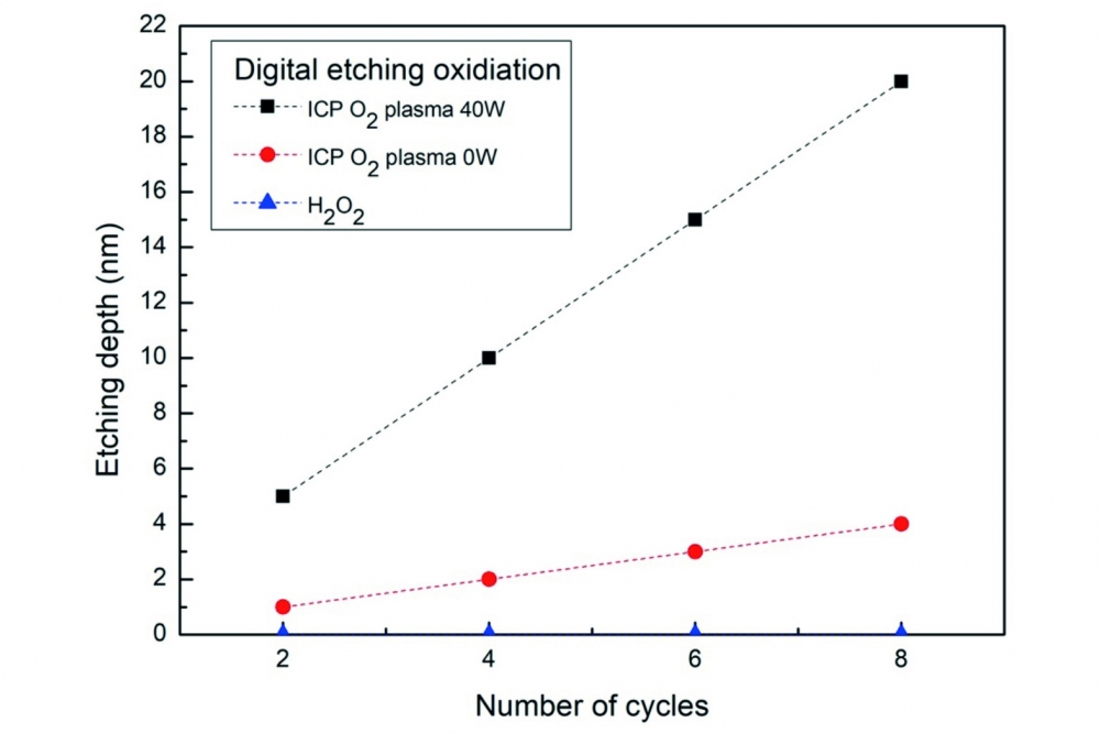
Atomic force microscopy measurements revealed good linearity in the etch depth per cycle (see Figure). Using RF powers of 40 W and 0 W, the average etch rates with the oxygen plasma treatment were 2.5 nm per cycle and 0.5 nm per cycle, respectively. The process involving hydrogen peroxide produced an etch depth per cycle close to 0 nm. Based on these findings, further studies were restricted to the use of oxygen plasma treatments.
X-ray photoelectron spectroscopy uncovered the presence of a strong peak associated with oxygen in samples subjected to plasma treatment. This peak’s strength plummeted after dipping the sample in HCl, demonstrating that this step provided good oxide removal.
Atomic force microscopy on 1 µm by 1 µm areas revealed that after three digital etch cycles, the AlGaN surface had a root-mean-square roughness of 0.10 nm and 0.09 nm for 40 W and 0 W treatments, respectively. Etching with a chlorine plasma increased the rougness to typically 0.49 nm.
The team produced HEMTs with a 110 nm gate length using three etching processes: one cycle, 0 W bias; six cycles, 40 W bias; and eight cycles, 40 W bias. Measurements with a 5 V drain bias showed that increasing the number of cycles, and thus the amount of material etched, led to a decrease in drain current and transconductance, along with a shift in the threshold voltage – it increased from -2.7 V to 0 V and then 0.4 V. The positive threshold voltage, crucial for normally off operation, came at the expense of drain current and transconductance, due to the creation of a very thin AlGaN barrier layer that almost ensured depletion of the two-dimensional electron gas.
Tsai said that the team might now refine its technique for use on larger wafers, so that it could be applied to high-volume production of RF devices with good uniformity.
REF
P. -Y. Tsai et al. Appl. Phys. Express 14 126501 (2021)


