Loading...
News Article

Soitec to expand manufacturing footprint

News

New Bernin fab will produce high volume SmartSiC wafers for EVs and industrial markets and increase SOI capabilities

Soitec has announced today a new fabrication facility at its headquarters in Bernin, France, primarily to manufacture new SiC wafers which respond to key challenges of the electric vehicle and industrial markets. The extension will also support Soitec’s 300-mm Silicon-on-Insulator (SOI) activities.

The factory is to produce innovative SmartSiC engineered wafers developed by Soitec at the Substrate Innovation Center located at CEA-Leti in Grenoble, using Soitec’s proprietary SmartCut technology.

Soitec says this new generation of SiC wafers adds significant value for industrial applications and electric vehicles. It allows to enlarge their driving range, shorten the charging time and diminish their cost. With its SmartSiC products, Soitec is engaged with major SiC device makers and targets to generate first revenues in the second half of calendar year 2023.

"We expect that by 2030, around 40 percent of all new cars will be electric. Our unique, highly performant, sustainable and cost competitive SmartSiC solution addresses the industrial challenges, helps to optimise energy efficiency, and will accelerate the adoption of electric vehicles," says Paul Boudre, Soitec CEO. "This investment is a major milestone for us as SmartSiC is set to be another growth engine for Soitec, and a driver of the transformation of the automotive and industrial markets."

Mitsubishi joins Horizon Europe's FLAGCHIP project
Vishay launches new high voltage SiC diodes
UK team leads diamond-FET breakthrough
GaN adoption at tipping point, says Infineon
BluGlass files tuneable GaN laser patents
QD company Quantum Science expands into new facility
Innoscience files lawsuit against Infineon
Riber revenues up 5% to €41.2m
Forvia Hella to use CoolSiC for next generation charging
Photon Design to exhibit QD simulation tool
Ortel transfers CW laser fabrication to Canada
Luminus adds red and blue multi-mode Lasers
PseudolithIC raises $6M for heterogeneous chiplet tech
Mesa sidewall design improves HV DUV LEDs
IQE revenue to exceed expectations
'Game-changing' VCSEL system targets clinical imaging
German start-up secures finance for SiC processing tech
Macom signs preliminaries for CHIPS Act funding
IQE and Quintessent partner on QD lasers for AI
EU funds perovskite tandems for fuel-free space propulsion
EU to invest €3m in GeSi quantum project
Transforming the current density of AlN Schottky barrier diodes
Turbocharging the GaN MOSFET with a HfO₂ gate
Wolfspeed launches Gen 4 SiC MOSFET technology
Report predicts high growth for UK's North East
Element Six unveils Cu-diamond composite
SemiQ launches hi-rel 1700V SiC MOSFETs
Lynred to exhibit Eyesential SWIR sensor for machine vision
Thorlabs buys VCSEL firm Praevium Research
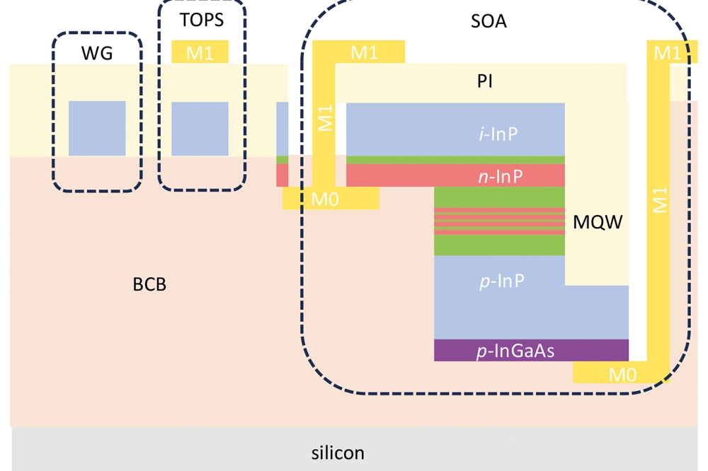
Advancing tuneable InP lasers on a heterogeneous platform
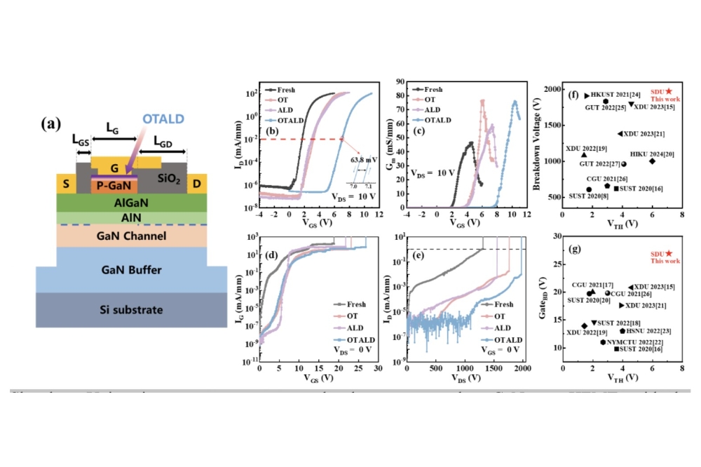
P-GaN gate HEMTs have record threshold voltage
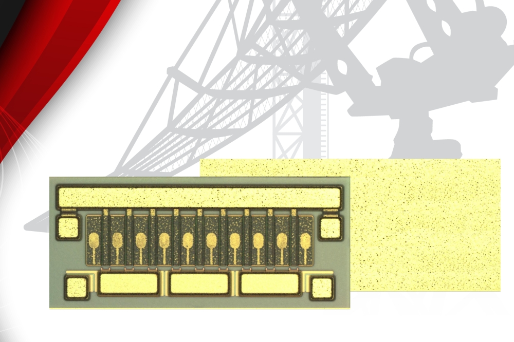
Guerrilla RF releases GaN power amplifier dice
×
Search the news archive

To close this popup you can press escape or click the close icon.
Logo
x
Logo
×
Register - Step 1

You may choose to subscribe to the Compound Semiconductor Magazine, the Compound Semiconductor Newsletter, or both. You may also request additional information if required, before submitting your application.


Please subscribe me to:


You chose the industry type of "Other"

Please enter the industry that you work in: