
Bristol University installs Gallium Oxide MOCVD system
Team expects to have first Ga2O3-based components within the next few months
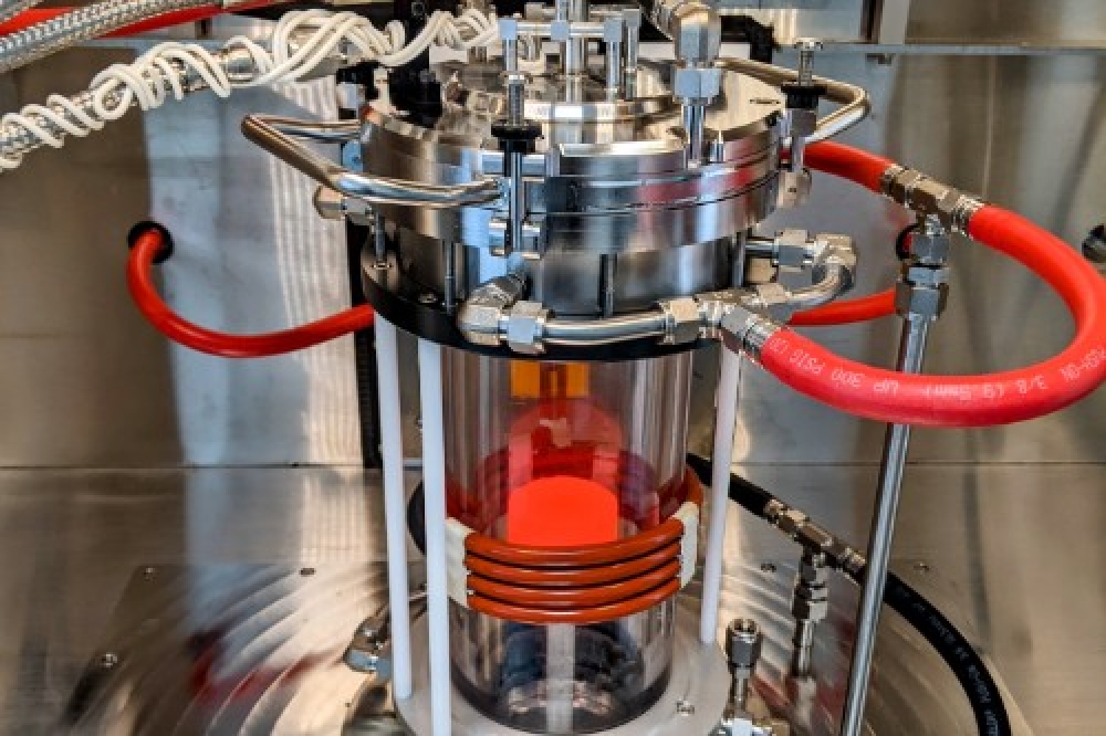
A team of scientists at Bristol University has just installed the UK’s first-ever MOCVD machine to make layers of Ga2O3, a compound semiconductor material that could help shrink power transformers the size of shipping containers down to the size of a suitcase
Project lead Martin Kuball, professor of Physics and Royal Academy of Engineering Chair in Emerging Technologies, said: “This is a hugely exciting and urgently needed opportunity. With the push to introduce more efficient power electronics and advanced renewable technologies amidst the pressing climate crisis, this presents a game changer for more sustainable and affordable future energy supply.
“At present nearly three-quarters (72 percent) of global primary energy consumption is wasted. While most low-carbon technology still relies on silicon-based electronic devices, we are slowly starting to see this replaced with semiconductors made from GaN and SiC. As action to reduce our carbon footprint accelerates, a stronger focus on developing devices based on Ga2O3 must happen and we are committed to progressing this at scale and speed.”
The 20-strong team of researchers is collaborating with other groups across the globe including in Japan, the United States, and Germany, as well as industry partners such as Dynex Semiconductors. Funded in part by the Royal Academy of Engineering, the Ga2O3 MOCVD system from Agnitron Technology in the US is the first of its kind in Europe.
“The MOCVD system will be used to grow thin layers, much thinner than a human hair, of Ga2O3 as well as Aluminium Gallium Oxide, in a chamber containing highly purified gases. These layers then go into our clean room, an almost entirely dust-free area, where metals and other layers are added, effectively electrical contact, to produce the finished power electronic component which is ready to use. These are even more energy efficient than current GaN and SiC components,” Kuball explained.
“We will be activating the machine this month and aim to have our first Ga2O3-based components within the next few months, putting us at the very forefront of making energy efficient power devices of the future.”
Kuball said: “Existing power converting units, often found in our streets, are container-size. Taking this technology to the next level could see them reduced to the size of a suitcase. You could then build distributed power networks, or smart grids, because the compact proportions make it possible to have more of them widely distributed. This would lower the risk of power outages for large parts of the town or city, as is presently the case when a power line goes down. The advantages of Ga2O3e-based technology are vast. Now more than ever we must develop and refine the processes to fully realise this.”


