
EVG to present 'More than Moore' technologies
Technical papers at IEEE ECTC in San Diego to highlight new developments around heterogeneous integration and wafer-level packaging
EV Group (EVG) will highlight new developments in heterogeneous integration and wafer-level packaging enabled by its lithography solutions in several papers at the 2022 IEEE 72nd Electronic Components and Technology Conference (ECTC), to be held May 31-June 3 in San Diego, Calif.
'Lossless High-speed Silicon Photonic MZI Switch with a Micro-Transfer-Printed III-V Amplifier' (Session 10, Novel Photonics Packaging Technology – Wed., June 1, 4:45pm) is a joint paper by EVG, Imec, the Photonics Research Group and the Tyndall National Institute.
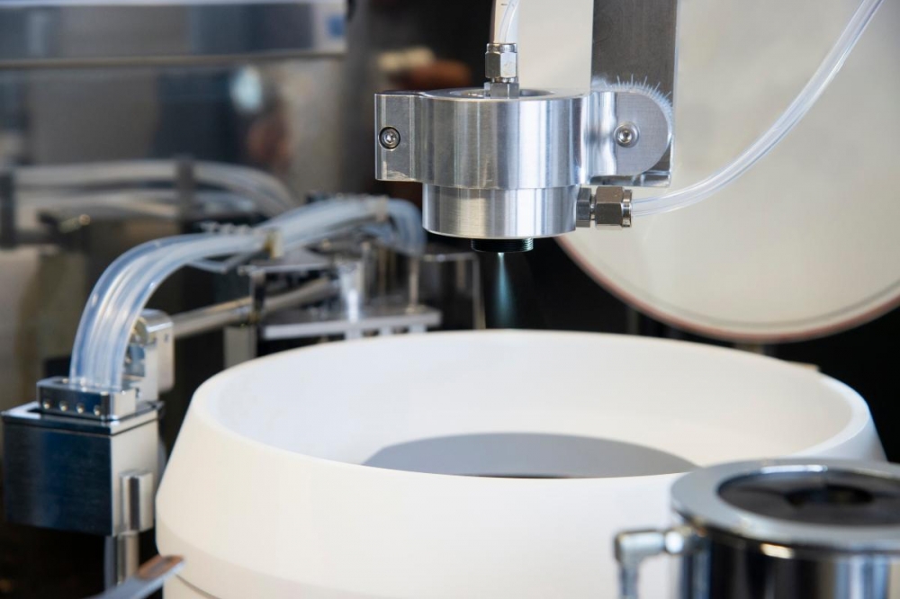
This first paper describes a novel approach for integrating III-V components on an advanced silicon photonics (SiPh) wafer through micro-transfer printing—enabling the economical and scalable integration of optical gain elements in photonic integrated circuits without modifying the established SiPh flow. To enable micro-transfer printing, an ultrathin bonding layer is applied to the source wafer by spray coating using EVG’s proprietary OmniSpray technology, which is said to provide excellent uniformity results on challenging topographies. (Pictured above is the OmniSpray module on an EVG120 automated resist processing system.)
'Optimization of PI and PBO Layers Lithography Process for High Density Fan-Out Wafer Level Packaging and Next Generation Heterogeneous Integration Applications Employing Digitally Driven Maskless Lithography' (Session 34, Processing Enhancements in Fan-Out and Heterogeneous Integration – Fri., June 3, 1:55pm) is a joint paper by EVG and Fujifilm Electronic Materials.
This second paper evaluates high-performance dielectric materials tailored for fan-out wafer-level packaging (FOWLP) using EVG’s novel LITHOSCALE maskless exposure lithography system, which allows for design flexibility and instant application of bias/offsets and optical proximity corrections at the die- and wafer-level. The ability to enable instant design alteration enhances final process results, such as resolution, via-footing and side-wall profile, while the mask-free approach of LITHOSCALE avoids yield issues associated with reticle stitching when patterning larger-area dies.
ECTC attendees interested in learning more about EVG and its suite of wafer bonding, lithography and metrology solutions for heterogeneous integration and wafer-level packaging are invited to visit EVG at its booth on May 31-June 3 at The Sheraton San Diego Hotel and Marina in San Diego.


