
Fraunhofer IAF revs up research infrastructure
New lab building and MOCVD hall will boost activities in optoelectronics, quantum technologies and materials science
Fraunhofer IAF has expanded its state-of-the-art research infrastructure and further improved the conditions for the development of pioneering semiconductor technologies.
With the support of the German federal government, the state of Baden-Württemberg as well as the BMVg, a laboratory building and an MOCVD hall were built, enabling the institute to intensify its activities in the fields of optoelectronics, quantum technologies and materials science. The official inauguration of the new buildings took place on June 30, 2022.
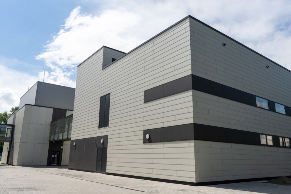
Two new research buildings provide researchers at the Fraunhofer Institute for Applied Solid State Physics IAF with the facilities they need to continue developing innovative technologies based on compound semiconductors at the cutting edge of technology.
With the new laboratory building for optoelectronic metrology and quantum sensing as well as the new facility hall for MOCVD, the institute lays the foundation for the continued strategic development of its core competencies. The new buildings meet high standards in terms of energy efficiency, sustainability and building dynamics. They were financed by funds from the German federal government, the state of Baden-Württemberg and the German Federal Ministry of Defense (BMVg) and were officially inaugurated on June 30, 2022.
The great benefits of the new buildings for the institute are explained by the head of research infrastructure, Martin Walther: “The new laboratories provide our scientists with even better research conditions. In particular, the application laboratories for quantum sensing and laser spectroscopy significantly expand the opportunities for cooperation with partners from industry and research.
"The new MOCVD hall has also enabled us to enlarge our epitaxy equipment park, further increase the level of material quality and reproducibility, and at the same time ensure significantly more efficient operation.”
Executive director of Fraunhofer IAF, Rüdiger Quay, also said: “I am very pleased that the buildings exceed the requirements of the German Energieeinsparverordnung EnEV (Energy Saving Ordinance) and feature CO2-neutral construction elements. This is an important signal for our plan to achieve climate neutrality by 2030 together with the Fraunhofer-Gesellschaft.”
The new laboratory building has a total of 22 laboratories on 900 m2 of floor space, which have been designed in terms of building dynamics for the use of highly vibration-sensitive equipment. They comply with the vibration limit lines B and C of the so-called Vibration Criteria (VC) and are thus suitable, for example, for the operation of microscopes with magnifications of up to 1000 times or lithography and inspection equipment with structure widths of up to 3 and 1 µm, respectively. In the long term, this ensures the use of demanding measurement technology for ever smaller structures and allows intensive research and development of quantum sensors such as scanning probe, wide-field and laser threshold magnetometers as well as laser-based sensor technology and innovative semiconductor lasers.
The newly constructed MOCVD hall provides space for five state-of-the-art systems, which will enable Fraunhofer IAF to expand its epitaxial activities in the field of high bandgap semiconductors in particular. The four existing systems, which were moved from the clean room of the main building, were joined by a new system specifically for the deposition of AlGaN with high aluminum content. The new plant reaches temperatures of up to 1400 °C, which has a positive effect on crystal quality and homogeneity. Advantages also result from the hall’s equipment, which has autonomous regenerative processing systems, enabling more energy-efficient and sustainable manufacturing processes


