
Innoscience Bi-GaN HEMTs used inside smartphones
OPPO announces world's first cell phones with inbuilt GaN charging protection
Chinese GaN-on-Si company Innoscience Technology has announced the Bi-GaN series of bi-directional GaN HEMT devices that save space and facilitate fast charging without suffering from the rises in temperature that can sometimes be seen in traditional silicon devices.
Innoscience has also revealed that mobile communications company, OPPO, is using the new BiGaN devices inside its phone handset to control the battery's charging and discharging currents. This is the first time that such protection, based on GaN technology, has been included in the phone itself – previously the circuitry had to be incorporated inside the charger.
The company says that one BiGaN HEMT can be used to replace back-to-back connected NMOS MOSFETs in a common-source configuration to achieve bi-directional switching of the battery's charging and discharging currents. This reduces on-state resistance by 50 percent, chip size by 70 percent, and temperature rise by 40 percent.
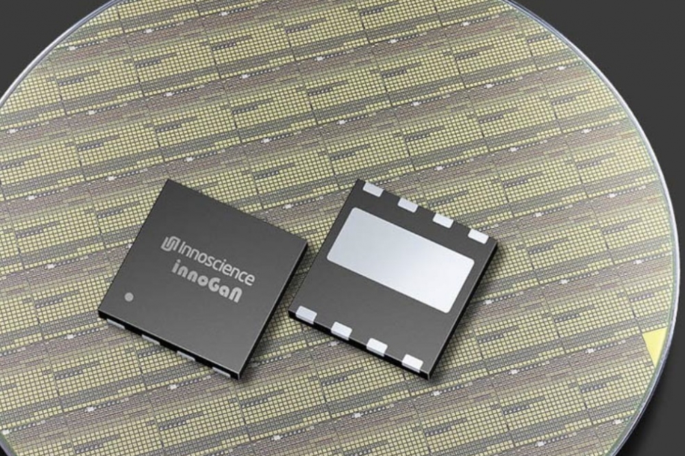
The first BiGaN device generally released by Innoscience is the INN040W0488, a 40V bi-directional GaN-on-silicon HEMT in the WLCSP package measuring 2.1mm x 2.1mm. The chip supports bi-directional switching with on-state resistance as low as 4.8mΩ. BiGaN targets applications such as overvoltage protection circuits for smartphone charging, high-side load switching circuits, and switching circuits for multi-power systems. Innoscience is also working to extend the bidirectional family to lower on-state resistance as well as to higher voltages.
At the recent UFCS Technical Seminar of the 1st Plug Conference of Guangdong, OPPO confirmed that it is using Innoscience’s BiGaN HEMTs inside handsets, making it the world's first cell phone manufacturer using BiGaN as direct charging load switcher. BiGaN products, said OPPO, not only save valuable space inside the phone but also reduce the temperature rise of the phone during charging.
This maintains a more comfortable temperature during fast charging, extends the possible duration of fast charging, and provides a better user experience. OPPO also announced that the BiGaN bi-directional technology will also be adopted in future volume production cell phone models. This is a significant development for the smartphone industry and the first time that GaN technology enters inside the mobile phone.
Comments Yi Sun, Sr VP of product development at Innoscience: “The application of BiGaN products inside smartphones marks the arrival of a new era for GaN. We are delighted and indeed honored that OPPO has announced it is using our innovative bi-directional HEMTs in their on-board fast charging circuit. We look forward to further collaboration to deliver solutions that deliver advanced performance.”


