
HKUST team develops way to couple III-V and silicon
Novel integration scheme uses selective direct epitaxy
Researchers at the Hong Kong University of Science and Technology (HKUST) has developed a novel integration scheme for efficient coupling between III-V compound semiconductor devices and silicon components on silicon photonics (Si-photonics) platform by selective direct epitaxy.
They say their method unlocks the potential of integrating energy-efficient photonics with cost-effective electronics, as well as enabling the next generation telecommunications with low cost, high speed and large capacity.
While silicon-based passive components have been well established on Si-photonics platform, the lasers and photodetectors can’t be realized by silicon and necessitate the integration of other materials such as III-V compound semiconductors on silicon.
III-V lasers and photodetectors on silicon has been investigated by two main methods. The first one is the bonding-based method which has yielded devices with impressive performance. However, it requires complicated manufacturing technique that is low yield and high-cost, making mass production very challenging. The other way is direct epitaxy method by growing multiple layers of III-V on silicon.
While it provides a solution with lower cost, larger scalability and higher integration density, the micrometers thick III-V buffer layers which are crucial for this method hinders efficient light coupling between III-V and silicon - the key for integrated Si-photonics.
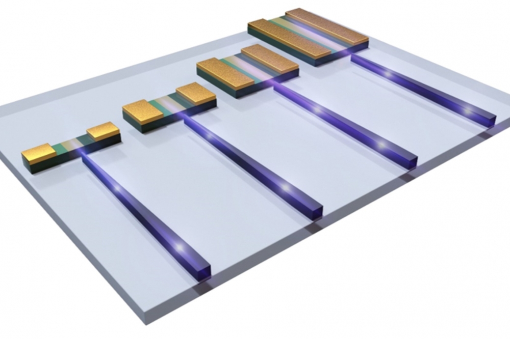
To address these issues, the team led by Kei-May LAU, professor emeritus of the Department of Electronic and Computer Engineering at Hong Kong University of Science and Technology (HKUST) developed lateral aspect ratio trapping (LART) - a novel selective direct epitaxy method that can selectively grow III-V materials on silicon-on-insulator (SOI) in a lateral direction without the need of thick buffers.
Furthermore, based on this novel technology, the team devised and demonstrated unique in-plane integration of III-V photodetectors and silicon elements with high coupling efficiency between III-V and silicon.
Compared to the commercial ones, the performance of photodetectors by such approach is less noisy, more sensitive, and has wider operation range, with record-high speed of over 112 Gb/s – way faster than existing products. For the first time, the III-V devices can be efficiently coupled with Si elements by direct epitaxy. The integration strategy can be easily applied to the integration of various III-V devices and Si-based components, thereby enabling the ultimate goal of integrating photonics with electronics on silicon photonics platform for data communications.
“This was made possible by our latest development of a novel growth technique named lateral aspect ratio trapping (LART) and our unique design of coupling strategy on the SOI platform. Our team’s combined expertise and insights into both device physics and growth mechanisms allow us to accomplish the challenging task of efficient coupling between III-V and Si and cross-correlated analysis of epitaxial growth and device performance,” said Prof. Lau.
“This work will provide practical solutions for photonic integrated circuits and fully integrated Si-photonics, light coupling between III-V lasers and Si components can be realized through this method” said Dr. Ying Xue, first author of the study.
This is a collaborative work with a research team led by Prof. Hon Ki Tsang of Department of Electronic Engineering at Chinese University of Hong Kong (CUHK) and a research team led by Xinlun Cai of School of Electronics and Information Technology at Sun Yat-sen University (SYSU).
The device fabrication technology in the work was developed at HKUST’s Nanosystem Fabrication Facility (NFF) on Clear Water Bay campus. The work is supported by Research Grants Council of Hong Kong and Innovation Technology Fund of Hong Kong. This work has recently been published in Optica.


