
III-V Lab counts on Riber MBE
Riber's MBE 412 allows the realisation of photonic and nanoelectronic components of the future
III-V Lab has chosen Riber's MBE 412 epitaxy equipment as part of the French Government scheme InPERIUM (InP for optoelectronic with Molecular Beam Epitaxy). "InPERIUM is a project implemented in the framework of the French recovery plan that allows us to increase our manufacturing capacity of wafers, components and optoelectronic and microelectronic modules for our strategic sectors,‘’ says Jean-Pierre Hamaide, president of III-V Lab.
III-V Lab is an Economic Interest Group between Nokia, Thales and CEA, dedicated to industrial research and development of optoelectronic and microelectronic components based on III-V semiconductors, and their integration with silicon circuits. Created in 2004, III-V Lab brings together 120 researchers in the Paris region and cooperates with CEA-Leti’s laboratories at Grenoble. III-V Lab has prototyping and production start-up resources to foster the emergence of high added-value component technologies which are then transferred to the industrial entities of the parent companies or their partners.
‘’The MBE 412 convinced us thanks to its reliability and its great modularity’’, explains Olivier Delorme, researcher in epitaxy at III-V Lab, ‘’Thanks to our understanding of physics of materials, combined with the versatility of epitaxy reactor, we explore many combinations of III-V semiconductors in order to develop high-performance components’’.
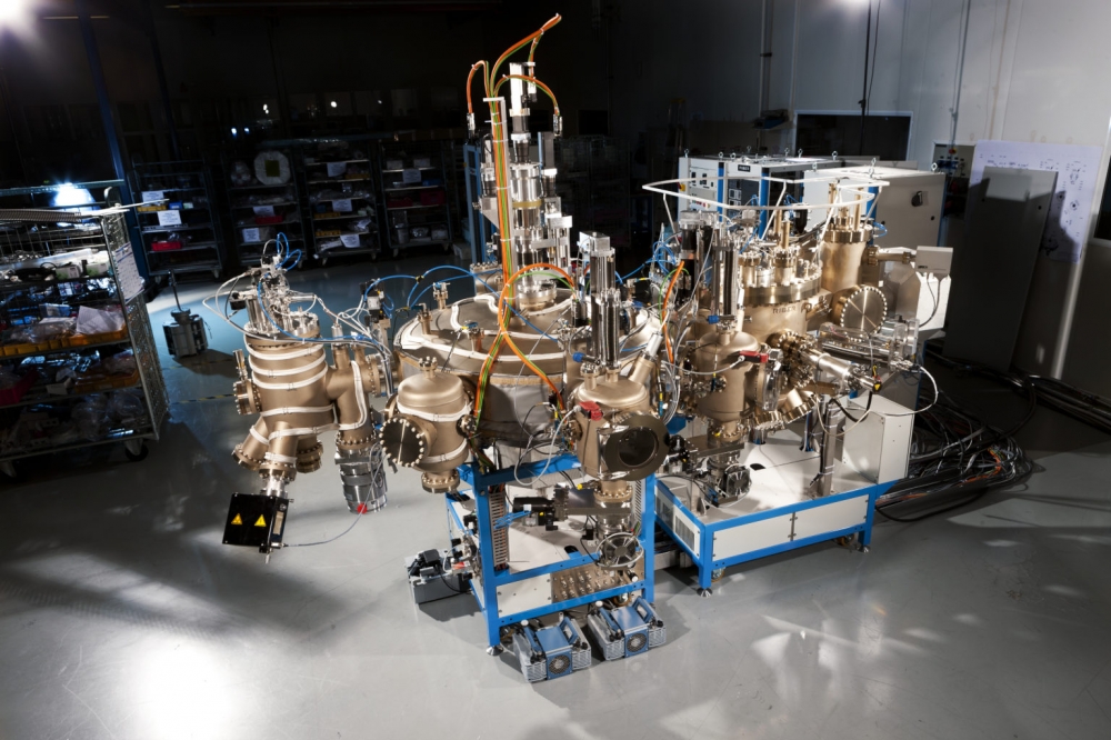
The cluster robot operating under ultra vaccum, allows to automatically transport wafers in different modules connected to the 8 available ports of the equipment. In particular, a preparation module, equipped with a hydrogen plasma source, has been installed improving the performance of components by providing optimum surface morphology.
Finally, the in situ characterisation instrument EZ-CURVE from Riber will be integrated and adapted for precise and continuous control of the growth process, thus contributing to a better control of the epitaxy processes allowing to improve the electronic or photonic performances and ultimately to increase the manufacturing efficiency of the components.
‘’Our MBE system cluster allows both product development and production. Our deposition reactor easily integrates various control instruments needed for the development of new materials. The modularity of the cluster design offers the opportunity to add additional reactors for pre/post process and analysis steps, or multiplying reactors to optimise product development and/or increase production efficiency. Our platform is fully automated and is driven by our software Crystal XE. Developed about ten years ago, the MBE 412 has been a worldwide success since then, with 25 operating systems worldwide and covering different applications: detectors, lasers, photovoltaic," concludes Michel Picault, chairman of the management board of Riber.


