
Passivating GaN with ruthenium
Schottky diodes deliver improved performance when a ruthenium solution is used to passivate the surface of GaN
A team from India is pioneering the use of a ruthenium solution to passivate the surface of GaN.
Effective passivation is crucial to optimising performance of GaN devices, as it eradicates defects such as oxygen impurities and nitrogen vacancies, causes of high gate-leakage currents.
The researchers – from Kurukshetra University, the University of Petroleum and Energy Studies and the Inter-University Accelerator Centre – have demonstrated the benefits of ruthenium treatment with GaN Schottky barrier diodes. Treated devices show considerably better performance, including a significant reduction in leakage current.
Spokesman for the team, Ashish Kumar, who is affiliated to both the University of Petroleum and Energy Studies and the Inter-University Accelerator Centre, told Compound Semiconductor that the team has been looking at the impact of ruthenium on GaN for many years. In 2014, they published a paper reporting the results of investigations with X-ray photoelectron spectroscopy; and now they are unveiling the findings of a study involving the use of scanning tunnelling microscopy and photoluminescence.
One of the benefits of using ruthenium for passivation is that it has a small atomic radius, which aids chemisorption on the GaN surface. A monolayer of ruthenium results from passivation, preventing atmospheric oxygen from forming bonds with gallium and nitrogen atoms.
“Ruthenium can have positive as well as negative oxidation states, so it can make stable bonds with both anions and cations,” explains Kumar, a claim confirmed by X-ray photoelectron spectroscopy, which revealed Ga-Ru and N-Ru bonds.
The latest study involved n-type, single-crystalline GaN with a thickness of 500 µm and a carrier concentration of 5.6 x 1017 cm-3, according to Hall effect measurements. Prior to passivation, samples were: ultrasonically cleaned in trichloroethylene, acetone and isopropanol, each for 10 minutes; rinsed with deionised water; dried under nitrogen gas; and etched in hydrochloric acid to remove the native oxide. Passivation resulted from dipping these pristine samples in a solution containing equal volumes of RuCl3 (0.05 M) and HCl (0.1 M).
Photoluminescence measurements on passivated and pristine samples revealed a doubling in the intensity of emission after treatment in ruthenium solution for 1 minute, and a small further enhancement when extending this process to 5 minutes.
Kumar and co-workers also used scanning tunnelling microscopy to compare passivated and pristine samples of GaN. Mapping areas of 62 nm by 62 nm revealed that ruthenium treatment altered the surface features.
Plots of tunnelling spectra – the current as a function of the bias voltage of the tip – showed that after chemical treatment, a dielectric layer is induced on GaN surfaces. This layer reduced tunnelling, and shifted behaviour at negative voltages, possibly due to a neutralising of defect states and the accumulation of charge carriers in the conduction band near the surface. The implication is that the position of the Fermi level changed, turning into the conduction band at the sample surface.
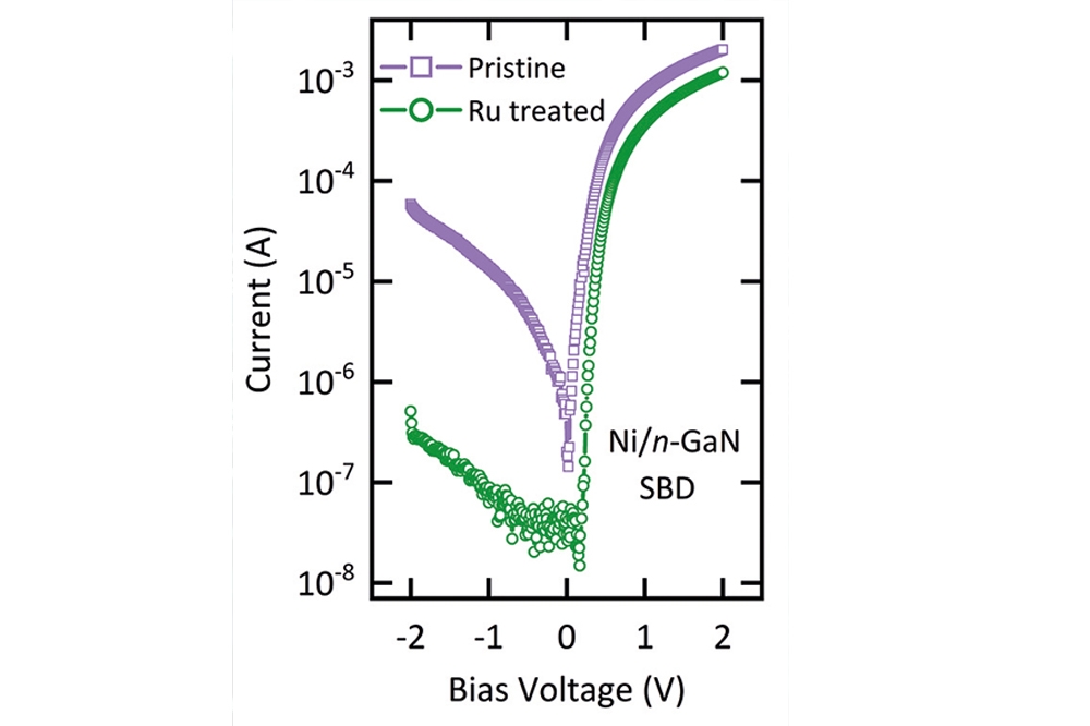
To demonstrate the effectiveness of their passivation process, Kumar and co-workers fabricated Schottky diodes on pristine GaN, as well as that subjected to ruthenium treatment. Measurements showed that passivation increased the Schottky barrier height from 0.78 eV to 0.91 eV, decreased the ideality factor from 1.42 to 1.12, and reduced the leakage current at reverse bias by around two orders of magnitude.
Kumar says that the team plans to continue its studies of passivation, using deep-level transient spectroscopy and time-dependent investigations.
Reference
N. Kumar et al. Appl. Phys. Lett 122 013503 (2023)
Pictured above: Current-voltage plots highlight the reduction in the leakage current provided by passivation with ruthenium.


