GaN transistors: An escalating patents war
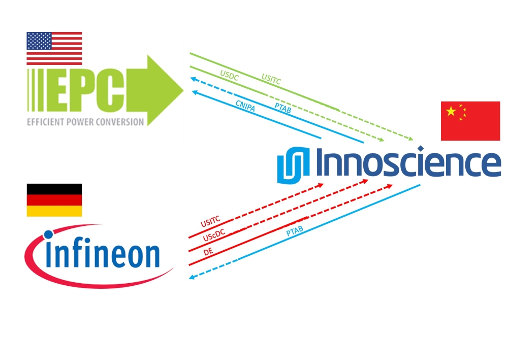
The battle over intellectual property surrounding the GaN power transistor is intensifying, with EPC and Infineon attacking Innoscience over patent infringement that it vigorously denies.
BY RICHARD STEVENSON, EDITOR, CS MAGAZINE
Within our industry, last summer will be remembered as the start of a global war surrounding the intellectual property (IP) of the GaN power transistor. Back then, Efficient Power Corporation fired the first shots, accusing Innoscience of infringing four of its patents. In only a matter of days Innoscience shot back, denying any wrongdoing. More recently, another company has entered the fray, with Infineon claiming that Innoscience is also not respecting its IP. And again, Innoscience is pleading innocence.
As claims and counterclaims are launched in courtrooms around the world, there is much value in hearing from those that combine expertise in this area with a neutral standpoint. Offering all this and more is David Radulescu, head of the patent litigation boutique firm Radulescu, who has been litigating semiconductor patents in courts throughout the US for three decades. More significantly, Radulescu also holds a PhD in compound semiconductor HEMTs and has previously devoted much effort to representing global companies fighting over IP associated with GaN-based LEDs.
In late July, Radulescu spoke for a second year in a row about the escalating IP war in a highly insightful webinar covering various patents that hold the key to deciding the outcome of the many court cases.
Before delving into details, Radulescu summarised the shots that had been fired to date: a pair of actions taken by both EPC and Innoscience in their battle, plus three fired by Infineon and another by Innoscience in their more recent skirmish.
This all kicked off last summer, when EPC announced it took legal action against Innoscience for infringing four of its patents. In the intervening months, EPC dropped two patents in its International Trade Commission (ITC) case, while initial rulings have been released on the other two this July. According to the administrative law judge (ALJ) in the ITC, both of EPC’s patents are not invalid, but significantly, he determined that one of them is infringed.
What’s also worth noting is that in the last couple of months action taken by Innoscience in China has also led to rulings that counterpart Chinese EPC patents were not invalid.
“We have Innoscience on its own turf losing in the Chinese Patent Office,” remarked Radulescu, who added that the US Patent and Trademark Office (USPTO) is still considering the validity of the patent found to be infringed by the ALJ, although the claims and prior art at issue are identical.
Radulescu offered a closer look at the key patents after highlighting the recent stockpiling of US patents issued to Innoscience. In the past year-and-a-half, the Chinese chipmaker was issued 45 US patents, while EPC was issued only one, leading Innoscience to outpace EPC in the total number of US patents by 58 to 57.
Gate designs
Focusing on the shape of the gate structure is EPC’s ‘508 patent, which the ALJ found to be not invalid but also not infringed.
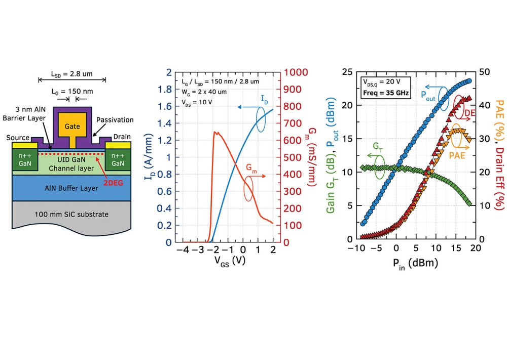
To put this patent in context, over the last few decades, a number of different gate structures have been used to produce GaN transistors, including: those that are self-aligned, with the gate and the insulator underneath having the same dimension (length); and those that have a T-shape or an inverted T-shape.
The ‘508 patent describes a multi-step process involving the use of three different photoresist patterns to produce a self-aligned gate.
For the claims brought by EPC concerning this patent, the key issue, according to Radulescu, is whether “etching away the doped GaN layer, except a portion of the doped GaN layer beneath the gate contact,” describes the Innoscience process.
“When you visually look at the [Innoscience] device, you see a gate ledge that is not co-extensive with the gate contact layer,” said Radulescu, who is not surprised that the ALJ viewed this transistor as being different from that of EPC, and thus concluding that there was no infringement.
The other important matter relating to the ‘508 patent is that Innoscience has asserted that it is invalid, an argument that was rejected by the ALJ.
Doping and compensation
Radulescu believes that those involved in ruling on the EPC-Innoscience battle will have a more difficult decision to make when it comes considering claims surrounding the ‘294 patent entitled ‘Compensated Gate MISFET’. In his view, what’s crucial is to understand what is meant by ‘compensated’, against the backdrop of the difficulties that have had to be overcome to realise p-type doping in GaN, key to producing LEDs with this material system.
The key claim by EPC is whether the phrase ‘compensated GaN layer’ describes the GaN layer in Innoscience’s devices that is presumed to be p-type based on its own publications.
It’s important to note, argued Radulescu, that EPC’s patent does not say anything about the GaN layer’s carrier type or its resistivity, characteristics that can be measured. Instead, it just uses the word ‘compensated’, a characteristic far harder to judge. This is because a picture or image of the device material is not determinative, but requires an understanding of semiconductor material science.
The other key point that Radulescu emphasised is that the ‘294 patent covers simply a transistor, and makes no reference to enhancement-mode or depletion-mode devices.
Many are assuming that the GaN employed by Innoscience is p-type. “They introduced magnesium, and I will be willing to bet that the hydrogen is intentionally removed after growth,” remarked Radulescu, whom added that secondary ion mass spectrometry (SIMS) plots have been disclosed during the case. “Whether or not you can call it ‘compensated’ depends upon how you define what compensation is,” added Radulescu.
Innoscience has argued that they do not employ a compensated GaN layer because they use a Schottky gate, as well as claiming that SIMS data reveals dopant activation, and testing confirms p-type conductivity. According to Radulescu, all these arguments were rejected by the ITC staff due to procedural errors of its counsel. For example, Innoscience offered evidence of the nature of the GaN through the testimony of an employee, an account viewed as problematic due to self-interest.
“Unfortunately for Innoscience, I don't think their best arguments were put forward,” commented Radulescu, who explained that the full Commission will now review the ALJ’s initial determination of infringement and issue a final decision on the investigation called a Final Determination, which is expected to issue in early November 2024.
Both Innoscience and EPC have tried to claim victory from the initial determination. Innoscience argues that it has won, because one of the patents was determined to not be infringed, while EPC is focusing on a finding of infringement.
The view of Radulescu is that while, in theory, EPC lost on three patents out of four, what really matters is that they have a ruling of a violation of the ITC statute against unfair competition by importing products that infringe US patents. And he believes that given how Innoscience’s lawyers argued their defences, it will be far from easy to get the ALJ’s determination reversed or modified, although not impossible.
Looking ahead, in March 2025, the US Patent Office will rule on the validity of the four patents asserted by EPC against Innoscience (which are also still at issue in EPC’s District Court case against Innoscience in California). If the ‘294 patent is determined to be invalid, this decision could be appealed, dragging the case on for a couple more years. Significantly, under this scenario, the ITC’s final determination will likely not matter as any potential importation ban would be expected to be stayed pending appeal. On the other hand, if the ‘294 patent is determined to not be invalid, and at the same time the full Commission agrees with the ALJ on infringement of the ‘294 patent, Innoscience’s products found to infringe would presumably be subject to some form of importation ban as that is a typical remedy available to patent owners in these type of ITC investigations.
Infineon versus Innoscience
Infineon’s actions against EPC began in March this year, when they brought a suit in San Francisco for a patent associated with high-voltage packages featuring so-called ‘source sensing’. Innoscience response to this has been to file a petition this June with the US Patent Office, arguing for invalidation of every single claim.
Meanwhile in Germany, Infineon has also filed several cases, as well as obtaining a preliminary injunction that prevented a small fraction of Innoscience’s high-voltage GaN transistors from being promoted at PCIM.
Commenting on this, Radulescu remarked: “Infineon outmanoeuvred Innoscience’s lawyers, because they got that injunction without Innoscience actually being heard on any of the issues. It was a surprise, but not unusual for parties to go to Germany to try to get these preliminary injunctions and mess up trade shows.”
Within the last few weeks, Infineon has stepped up its action, adding three more patents to the San Francisco case, and filing its own complaint with the ITC.
On the merits, the first of four Infineon patents that have been asserted involves an additional connection to the source of the power transistor, so that the parasitic elements associated with the packaging and connections have a reduced impact on overall system performance.
Infineon’s accusations centre on Innoscience’s use of a Kelvin source that it claims practices the patented source sensing functionality, as well as an identical pin layout. Like Infineon’s products, those in question from Innoscience have 8 pins, including one that’s a Kelvin source sensor.
Regarding the three other patents, one is concerned with the thickness of a titanium nitride capping layer in an electrode stack. The other two concern so-called 'merged cascode transistors', with one patent concerned with adding curvature to inter-digitated fingers to trim the electric field strength at the edge of the electrodes, and the other associated with combining a depletion-mode transistor with an enhancement-mode transistor to make a circuit. If the case is not settled beforehand, the ALJ’s initial rulings on these patents are not expected until autumn 2025.
While it is impossible to predict the rulings of all the asserted claims to date in the GaN patent war, there is no doubt that substantial time and money will be spent over the next few years trying to defend IP and the products based on them. There are many different outcomes that could emerge, including licensing deals and import bans – but what is for sure is that interesting times lie ahead.