Mastering the manufacture of HEMTs with an AlN buffer
A US collaboration is making tremendous strides towards the commercialisation of AlN/GaN HEMTs with an AlN buffer, grown on SiC substrates.
According to the team from Soctera and Qorvo, this class of HEMT has the capability to produce higher output powers at high frequencies than its conventional counterpart that’s based on the GaN-buffer, making it an attractive candidate for providing faster communication at gigahertz frequencies. However, up until now, demonstrations of AlN/GaN HEMTs grown on SiC substrates and featuring an AlN buffer have tended to be provided by academic research laboratories, and involve small pieces of substrate.
Addressing this limitation, engineers from Soctera and Qorvo have produced AlN/GaN HEMTs with an AlN buffer and an ultra-thin barrier on SiC substrates using a 150 mm GaN foundry process. These transistors, which have several impressive characteristics, promise to provide the foundation for Soctera to start sampling bare die HEMTs by the end of this year.
According to spokesman for the team, Soctera co-founder and CTO Reet Chaudhuri, his company’s contributions have included epitaxial layer design and the epitaxy of the HEMT structure on SiC wafers.
“Qorvo performed the fabrication of the devices using Soctera’s epitaxial wafers, utilising their expertise from their 150 nm RF GaN technology,” remarked Chaudhuri. “This highlights a strong collaborative effort in advancing the technological readiness of the AlN/GaN/AlN HEMTs.”
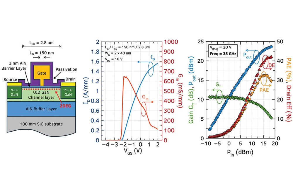
Fabrication of the collaboration’s metal-polar heterostructures began by loading 100 mm SiC substrates into an MOCVD reactor and growing an AlN buffer layer, a GaN channel layer that’s less than 200 nm-thick, and a 3 nm-thick AlN barrier layer. None of these layers featured any intentional doping. It’s argued that the heterostructure is unlikely to be pseudomorphic, due to a partially relaxed GaN channel layer.
Electrical measurements of the epiwafers determined that the two-dimensional electron gas (2DEG) has a density of 1.26 x 1013 cm-2, a mobility of 1248 cm2 V-1 s-1, and a sheet resistance of 442 W sq-1. Across the epiwafer, variation in sheet resistance is just 1.5 percent, indicating a high level of uniformity that enables this material to provide a good foundation for electronic device fabrication.
The team processed their epiwafers into HEMTs with a 150 nm gate length that included re-grown GaN contacts for the source and drain and a Schottky gate electrode defined by electron-beam lithography (see figure for more details).
Characterisation of the HEMTs determined: an ohmic contact resistance of 0.09 W mm; an on-off ratio for the drain current of around 106; a peak transconductance of 643 mS mm-1; and normally-on behaviour, with a pinch-off voltage of about -2 V, defined as the gate voltage at a drain current of 1 mA mm-1. Stressing the device for 1 hour at a drain-source voltage of 20 V produced a 10 percent permanent degradation in drain current. Evaluation of large signal amplification determined a power-added efficiency of 32 percent and an output power density of 2.68 W mm-1.
Reet argued that the ultra-low contact resistance and extremely high transconductance of these HEMTs provides a fantastic foundation for building millimetre-wave power amplifiers.
“To translate these metrics to higher output power at Ka-band, reduction of current collapse will be key, which will involve optimisation of the passivation technique for this specific epitaxial structure.”
According to Chaudhuri, Soctera will continue to devote efforts towards developing GaN power amplifiers that outperform today’s products, in terms of delivering higher powers at cooler operating temperatures. “Our first product devices are going through the production foundry right now, and we anticipate providing samples to interested customers by the end of 2025.”
Reference
R. Chaudhuri et al. Appl. Phys. Express 18 076501 (2025)