Scientists develop tiny UV spectrometer
The iGaN Laboratory led by Haiding Sun at the University of Science and Technology of China (USTC) together with a team from Wuhan University, Zhejiang University and the University of Cambridge, has developed the first miniaturised ultraviolet (UV) spectrometer and realised on-chip spectral imaging.
Based on a novel GaN cascaded photodiode architecture and integrated with deep neural network (DNN) algorithms, the device achieves high-precision spectral detection and high-resolution multispectral imaging. With a response speed on the nanosecond scale, it sets a new world record for the fastest reported miniaturised spectrometer. The work was published online in Nature Photonics on September 26, 2025.
Spectral imaging technology captures both spectral and spatial information simultaneously, enabling the precise measurement and identification of complex environments and targets. It has wide applications in material analysis, environmental monitoring, satellite remote sensing, and deep-space exploration.
However, conventional spectral imagers rely on diffraction gratings and mechanical scanning, making them large, complex, and costly, and limiting their portability and integration. In particular, for deep-UV/UV applications crucial in biopharmaceuticals and organic molecule detection there has long been no viable solution.
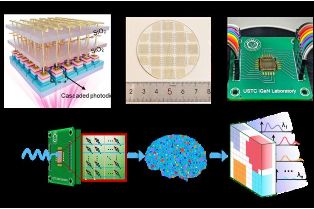
To overcome this challenge, the iGaN Laboratory proposed a new GaN-based cascaded photodiode architecture and developed the first UV spectral imager.
The structure consists of two vertically cascaded asymmetric p–n diodes that can be fabricated as arrays on 2-inch wafers and integrated through bonding. By applying external bias, carrier transport exhibits wavelength-dependent behaviour, enabling voltage-tuneable bidirectional spectral response. With the aid of DNN algorithms , the device reconstructs unknown spectra with high accuracy.
Operating across 250–365 nm, the device achieves ~0.62 nm resolution and <10 ns response time the fastest among all reported miniaturised spectrometers.
Using this device, the team successfully performed spatially resolved, single-shot imaging of organic liquid droplets, including olive oil, peanut oil, animal fat, and milk. Each pixel recorded wavelength-dependent photocurrent signals, generating a full three-dimensional dataset.
After spectral reconstruction via neural networks, high-resolution spectral images were obtained, clearly showing the distinct UV absorption characteristics and spatial distributions of different organic substances. These demonstrations highlight the device’s potential application in molecular recognition and food safety testing.
The team says the work presents and validates a new paradigm for miniaturised spectrometer/spectral imager and, for the first time, uses wide-bandgap nitride semiconductors for building such devices.
Looking forward, by adjusting material composition and doping, or by introducing other compound semiconductors (such as CdS, ZnO, GaAs, and InP), the operational range of this device architecture could be extended from UV to visible and even infrared.
Because the fabrication process is fully compatible with large-scale semiconductor manufacturing, the device dimensions can be further reduced to submicron or nanometer scales, enabling higher resolution at lower cost.
The team anticipates that production costs could fall to as little as one-hundredth that of conventional spectrometers. Much like silicon-based CCD/CMOS technology enabled the widespread adoption of digital cameras, this GaN-based miniaturised on-chip spectrometer is poised to drive a new wave of industrial advancement in spectral imaging technology.