What does the future hold for the compound semiconductor industry?

Growth is forecast for all leading forms of compound semiconductor
device, driven in part by demand for more data, an uptake in AI,
increasing opportunities for satellite communication and growing sales
of electric vehicles.
BY ALI JAFFAL, TAHA AYARI AND AYMEN GHORBEL FROM YOLE GROUP
THE COMPOUND SEMICONDUCTOR industry is now booming, having established itself as a significant player alongside silicon-based semiconductors, bringing not only superior performance but also new functionalities that silicon cannot achieve, such as light emission. These semiconductors are becoming increasingly popular in power electronics, RF, photonics, and microLED displays. For power applications, sales are dominated by SiC and GaN devices; for RF applications, GaAs and GaN devices lead the way; for photonics, InP and GaAs are the leading material systems; and for LED/display applications, GaAs and sapphire are the key substrate materials.
The compound semiconductor industry is well-established, having formed an entire ecosystem, with its own equipment for crystal growth, wafer manufacturing, front-end manufacturing, testing and packaging. According to recent market research by our company, Yole Group, the value of compound semiconductor substrates is rising at a compound annual growth rate of 17 percent over the 2023 to 2029 timeframe, to reach US$3.3 billion1. Underpinning this growth is an expansion in key facilities that are supporting a transition to larger substrates. There is a migration to 200 mm wafers for SiC and GaN-on-silicon, driven by power electronics growth in the automotive and consumer markets; in the photonics sector, the use of 150 mm InP is on the rise, spurred on by the datacom market; and in the microLED displays market, there is increasing use of 200 mm GaAs and sapphire. However, the latter application has been hit badly by Apple, who closed its microLED project earlier this year, after being the main player pushing for 200 mm substrates with it partner ams-Osram2.
Looking in more detail at the substrate market, a number of SiC substrate makers, including Coherent, Wolfspeed, SK Siltron, SICC and TankeBlue, are actively working on the 200 mm format, with initial volume shipments starting late last year. The Chinese SiC substrate supply is growing rapidly, and is fiercely competing with the US8.

For GaN-on-silicon for power applications, for the last 2-3 years volume production has involved 200 mm wafers, the format employed by the massive Chinese company Innoscience. All recent investments and capacity expansions are focused on this platform, including Infineon’s GaN fabs in Villach and Kulim.
When it comes to InP, the mainstream substrate size is still 75 mm. However, market leaders such as Sumitomo Electric and AXT have the capability to produce good-quality 150 mm InP substrates, and this year they are shipping significant volumes for R&D. Sales of higher volumes are expected over the next few years.
Regarding GaAs, 150 mm substrates continue to dominate photonics and RF applications. Here the market is dominated by Sumitomo Electric and Freiberger.
As well as high-quality substrates, optimal devices demand high-quality epitaxy. This leaves chipmakers with one of two choices – to adopt the captive approach, and undertake epitaxy in-house; or to use an ‘open’ approach, drawing on the epitaxial services of a number of players, including IQE, Landmark, VPEC, IntelliEPI and Sumitomo Chemical. We estimate that between 2023 and 2029 the open epiwafer market will expand at a compound annual growth rate of 19 percent to hit US$2.5 billion. Sales from the SiC open epiwafer market are already soaring, and will climb to account for 64 percent of that total by 2029.

2023-2029 compound semiconductor substrate market by application ($M). Source: Status of the Compound Semiconductor Industry report, Yole Intelligence, 2024. Credit: Yole Intelligence
EVs and fast chargers are gaining
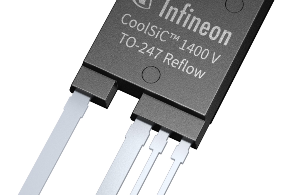
Since 2017-2018, sales of SiC and GaN devices have experienced rapid growth. Helping this has been Tesla’s adoption of SiC in its inverters, a move that marked significant disruption in the EV market. Here SiC plays a crucial role in 800 V fast charging, significantly reducing the time it takes to accomplish this task. Today, high-volume EVs, such as BYD’s Han and Hyundai’s Ioniq 5, are being shipped with SiC technology. Sales to automakers have ramped the revenue of leading device manufacturers like STMicroelectronics, onsemi, Infineon, Wolfspeed, and Rohm. These pioneers of high-volume SiC power device production all realised record revenue in 2023, and are on track to net sales from these products of US$1 billion by 2024-2025. We forecast that by 2029 the total market for SiC devices will exceed US$9.6 billion3, with ramping revenue not only driven by the EV market – sales growth will also come from industrial, energy, and rail applications. Supporting this substantial hike in revenue is capacity expansion, business integration, and innovative business models.
Meanwhile, in the power GaN market the primary drivers of growth are still consumer applications. Recent trends include chargers with higher power capacities of up to 300 W, along with power supplies and motor drives for home appliances that offer a higher efficiency and compactness.
We are foreseeing two additional catalysts for power GaN growth: automotive and data-centre applications. Due to these contributions, the power GaN market will be propelled to more than US$2.25 billion by 20293.
Evolutions in RF
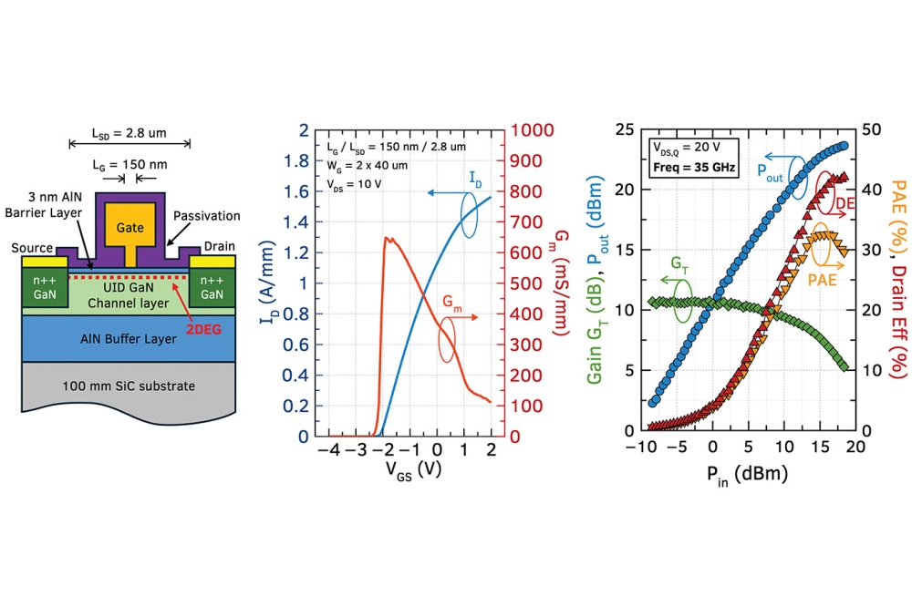
In the RF domain, GaAs technology is a well-established building block for RF front-end modules in smartphones, and is showing growth opportunities in automotive applications. The other key material in RF is GaN-on-SiC. Over the last two decades this has been used to develop power amplifiers for defence and aerospace applications, with efforts given much support by the US government. With the advent of 5G, new macro base stations are adopting GaN technology over existing silicon LDMOS, a move that enables more complex architectures at higher frequencies with greater efficiency. RF GaN technology is also expanding into markets such as satellite communication and RF energy. According to our recent analysis, the total RF GaN device market will grow from US$1.1 billion in 2023 to US$2.07 billion by 20294,7.
An alternative material system for RF devices that has garnered interest in recent years is GaN-on-silicon. Last year Infineon introduced a GaN-on-silicon power amplifier module processed on 200 mm wafers to the telecom infrastructure market, directly competing with GaN-on-SiC technology. With the potential to scale to 300 mm, RF GaN-on-silicon could offer performance and cost benefits to compete with GaAs technology for 6G PAs. Other companies exploring RF GaN-on-silicon technology include UMC, STMicroelectronics, GlobalFoundries, Sony and Finwave. As these newcomers invest in power GaN-on-silicon, they are able to use 200 mm facilities to enter RF applications without having to make risky investments.
A pioneer of 150 mm RF GaN-on-silicon technology is Macom. This US chipmaker has secured design wins for military tactical radios for over a decade. Last year Macom expanded into satellite communication by acquiring Ommic SAS, and enhanced its GaN-on-SiC portfolio by buying Wolfspeed’s RF business. These acquisitions have elevated Macom to one of today’s top four RF GaN device players.

Evolution of compound semiconductor applications– inflection points. Source: Status of the Compound Semiconductor Industry report, Yole Intelligence, 2024. Credit: Yole Intelligence
AI drives photonics growth
The other major applications within the compound semiconductor industry are based on photonics. A significant market here is the GaAs VCSEL for 3D sensing in smartphones. This application began in 2017 with Apple, followed by Android makers like Huawei and Xiaomi. While US-China sanctions have slowed uptake, there has been a re-adoption of GaAs VCSELs for 3D sensing, with Chinese OEMs such as Huawei, in this case using this technology in its Mate 60 Pro model. This leads one to wonder whether we will now see more Chinese OEMs adopting GaAs VCSELs in the consumer market – and whether these chipmakers will be able to meet the cost target for low-end smartphones. What is beyond question is that GaAs VCSEL supply is growing in China, with several players demonstrating excellent capabilities, including Vertilite, Everbright photonics, RaySea, and QM lasers. This expertise will aid the adoption of VCSELs for automotive lidar in China. Note that China represents the biggest market for automotive lidar.
In the optical communications sector, AI is driving GaAs VCSEL adoption in data centres. These emitters are being deployed in optical transceivers that transmit and receive data at 800G and beyond. Key to such high speeds are 100G/lane VCSELs. Coherent and Broadcom are already mass-producing these devices, and Lumentum is set to follow later this year. Development of 200G/lane VCSELs for 1.6Tb pluggables is underway, with mass production forecast for 2026-2027. This begs the question: What technology will be used in 1.6Tb optical transceivers for short-reach applications between 2024 and 2026?
Also driven by AI are sales of InP edge-emitting lasers, with shipments to this application dominated by 100G and 200G/lane InP electro-absorption-modulated lasers and high-power continuous-wave distributed-feedback lasers that are enabling 800G and 1.6T optical transceivers in long-reach applications.
Back in 2023, AI had yet to make a significant impact, and that year was a challenging one for the InP business. Headwinds came from a slowdown and increased inventories from hyperscalers and cloud service providers, as well as reduced consumer market adoption when Apple reverted to the GaAs VCSEL for proximity sensors, instead of using InP edge-emitting lasers.
Since the beginning of this year, the situation in the InP market has improved significantly. This is especially true for the datacom sector, which is driving growth in substrates, epiwafers, and devices. Several encouraging signs have emerged, such as Lumentum’s acquisition of Cloudlight to ensure full vertical integration in its datacom business. However, the most significant development is the announcement of a 150 mm InP fab at Coherent. Will we now see other players adopting the 150 mm InP platform to reduce costs and meet market demand, especially if InP re-enters the consumer market in the short term and 6G in the long term?
After weighing up all the likely scenarios, we forecast that the GaAs and InP photonic bare die markets will reach US$1.94 billion and US$.3.5 billion, respectively, in 20295.
What’s next?
To push performance and cost limits, the compound semiconductor industry continues to explore new materials, platforms and designs. Now one critical question is this: Which emerging semiconductor substrate will be the next game changer? The answer is not obvious, as material scientists and industrial players are developing a number of new foundations for epitaxial growth, including Ga2O3, diamond, bulk GaN, GaSb, InSb, bulk AlN, smart-SiC, and an engineered substrate based on polycrystalline AlN. We are projecting that the emerging substrate market will grow to US$264.5 million by 20286, driven by power applications, particularly using engineered substrates.
Considering all these advances, the compound semiconductor market is set for sustained growth, especially in sectors where silicon falls short. The future of technology will undoubtedly be shaped by the ongoing evolution and impact of compound semiconductors.