

Infinitesima enters next growth phase
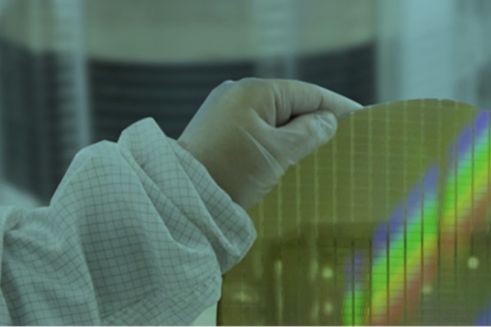
Infinitesima, a UK company developing advanced metrology tools, is continuing to scale its technology for high-volume semiconductor manufacturing.
This includes appointing David Reynolds as senior director of engineering. He was previously director of engineering at Nordson Test & Inspection, where he led an 80-person engineering organisation across the UK, Germany and India developing advanced X-ray metrology systems.
The company has also hinted at the possibility of applying its technology (currently configured for 300mm wafers) to compound semiconductors.
Infinitesima has developed a fundamentally different atomic force 3D surface measurement technique, the Rapid Probe Microscope (RPM). This combines thermal-optical actuation with an interferometric measurement system delivering picometer precision and speeds >100x faster than those achievable with conventional Atomic Force Microscope systems. RPM enables detailed 3D measurement of advanced semiconductor structures used in High NA EUV lithography, advanced packaging, hybrid bonding and next-generation semiconductor devices.
Its tools today are targetted at high-volume 300mm manufacturing (supporting customers including SK hynix, and involving collaborations with Imec and ASML) but Infinitesima says the technology could equally be applied to compound semiconductors.
"It’s certainly an area we see potential to move into in the near future, based on market demand", a company spokesperson told Compound Semiconductor. "The underlying technology and applications would be the same for compound semiconductors. If there is sufficient demand from the compound semiconductor market, the tool can be adapted to accommodate different wafer sizes without changing the core technology."



