
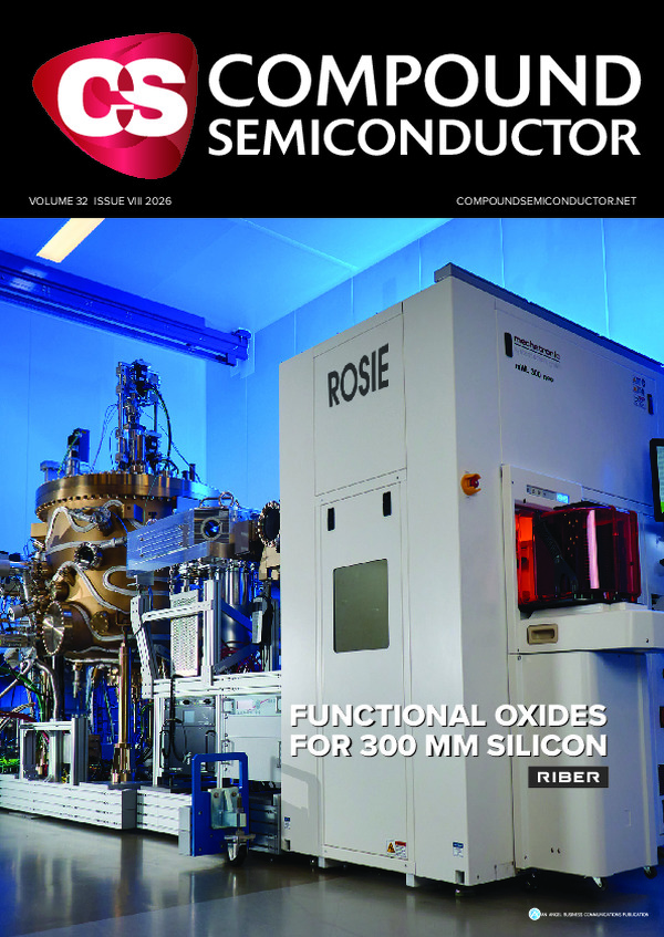
Functional oxides for 300 mm silicon

Silicon photonics and quantum computing will benefit from Riber’s recent MBE platform, which supports the growth of oxides on 300 mm silicon.
BY CLAUDINE PAYEN FROM RIBER
We are living in an era experiencing a rapid growth in data traffic, driven by cloud computing, artificial intelligence and high-performance computing. Due to these trends, optical interconnects in data centres must improve, to satisfy demand for higher data rates, lower power consumption and greater integration density.
Key to addressing all these goals is a critical building block in the transmission chain, the electro-optic modulator – it converts electrical signals from electronic circuits into optical signals, which are subsequently transmitted down fibre at very high data rates. Much effort is directed at improving the performance of these modulators, which ideally combine a very high bandwidth with minimal power consumption, low drive voltage, low optical losses and high integration density, while remaining compatible with large-scale manufacturing processes.
One of the most attractive platforms for addressing this challenging list of requirements is silicon photonics. However, this material system has a fundamental limitation for electro-optic modulation: it fails to offer a significant intrinsic linear Pockels electro-optic effect. Due to this shortcoming, there is much interest in integrating materials that address this weakness head-on to overcome some of the limitations of conventional silicon modulators.
Among the various electro-optic materials under investigation, one with a particularly strong potential is barium titanate, which has the chemical composition BaTiO₃, and is often referred to as BTO. It is classed as a ferroelectric oxide, has a perovskite crystal structure, and exhibits high electro-optic coefficients.
When evaluating the promise of any material for electro-optic modulation, two key considerations are the voltage and the interaction length required to achieve a given phase shift. The desire for a low voltage, or a short interaction length, is captured by a metric known as the VpL product. When BTO modulators are integrated on a silicon photonics platform, the value for VπL can be as low as 0.2 V cm, realised alongside modulation at 25 Gbit s-1.
Unfortunately, high Pockels coefficients do not guarantee a high-performance for an integrated modulator – a number of scientific and technological challenges must also be addressed before BTO can be deployed on a large scale.
One hurdle concerns material quality; and in particular, the crystalline quality of thin films, and the control of their ferroelectric domains. The electro-optic response of BTO depends strongly on crystallographic orientation, strain state and the ferroelectric domain configuration. Due to this, it is critical to control these parameters across the wafer, as this is needed to realise high, uniform and reproducible performance.
A second challenge relates to the integration of BTO with silicon photonics platforms. Currently under investigation are a variety of strategies, including epitaxial growth. Can any of these approaches combine high crystalline quality with integration schemes compatible with silicon photonics manufacturing?
Opportunities in quantum tech
The excellent electro-optic properties of BTO ensure that this material is a promising one for quantum technologies, and in particular, quantum computing architectures operating at cryogenic temperatures. A key building block in this sphere is the superconducting-qubit processor, which manipulates quantum information in the microwave domain. Since optical photons are far better suited to the transmission of information over long distances, there’s a need to develop interfaces between these two domains. Success is critical to advancing interconnected superconducting quantum processors that will ultimately enable distributed quantum computing.
With quantum architectures, electro-optic properties could make valuable contributions at several levels. That includes electro-optic modulators operating at low temperatures, as this enables the generation, routing and modulation of optical signals directly within a cryogenic environment. This technology is particularly attractive for the development of cryogenic photonic circuits, which could interface low-temperature systems with instrumentation operating at room temperature.
Note that BTO is especially promising in this context, as it retains its strong electro-optic response at cryogenic temperatures.
From material control to device performance
Datacom and quantum applications share a common challenge: controlling the properties of BTO, to ensure a reliable, reproducible device performance. In this context, MBE is a particularly attractive approach. This class of epitaxy enables growth of thin films while ensuring very precise control of thickness, composition and interfaces. Thanks to the independent control of elemental fluxes, ultra-high-vacuum growth conditions and the use of in situ characterisation techniques such as RHEED, with MBE it’s possible to monitor and optimise the earliest stages of growth.
This level of control is critical when integrating BTO on silicon. During the growth of perovskite oxides directly on silicon, there’s the threat of an amorphous SiO₂ layer forming at the interface, and preventing epitaxial growth. To avoid this, engineers can insert a strontium titanate (SrTiO₃ or STO) buffer layer between silicon and BTO.
A team at Oak Ridge National Laboratory pioneered this approach. Many years ago, they demonstrated that precise control of the first monolayer enables epitaxial integration of perovskite oxides on silicon. Following engineering of the interface between silicon and STO, the latter provides a crystalline perovskite surface suitable for epitaxial growth of BTO.
Don’t dismiss this STO buffer as just an intermediate layer: the oxide provides a key interface between silicon and the electro-optic material. Its crystalline quality, stoichiometry, and the structure of the interface between STO and silicon influence the orientation, defect density and strain state of BTO grown on top. Since these parameters are directly linked to the ferroelectric and electro-optic properties of BTO, it is a key technological challenge to control STO nucleation and growth.
With MBE, engineers enjoy precise control of the entire growth process, from silicon surface preparation through to the epitaxy of the STO buffer and BTO layer. These growers benefit from accurate control of the interfaces, stoichiometry, crystal structure and strain of the BTO/STO/silicon heterostructure.

ROSIE is equipped with mandatory in-situ instruments, providing curvature and reflectivity measurements.
ROSIE: a 300 mm silicon platform
Building on our patented reactor that’s designed for oxide epitaxy, our company, Riber, has developed a platform for integrating functional oxides on silicon wafers. Our goal has been to combine the precise control of MBE with the requirements of the semiconductor and silicon photonics industries.
Our efforts led to the launch of ROSIE, which is short for Riber Oxide Silicon Epitaxy. It’s a platform designed for the growth of functional oxides on 300 mm silicon wafers.
One feature of ROSIE is its architecture: front-opening unified pod to front-opening unified pod. This enables 300 mm wafer handling in an environment that’s suited to silicon manufacturing requirements.
With the introduction of ROSIE, the objective is no longer simply demonstrating the outstanding properties of BTO on laboratory-scale samples. Now the aim is to develop and qualify processes directly relevant to industrial semiconductor infrastructure.

One of the first TiO2-on-silicon 300 mm wafers demonstrating excellent thickness uniformity.
Connecting materials and devices
To qualify ROSIE within a structured scientific environment and establish a direct link between material growth and device performance, we are playing our part in a three-year collaboration that also involves the Novo Nordisk Foundation Quantum Computing Program (NQCP)/Niels Bohr Institute (NBI) in Denmark. Our initiative is called POEM, which is short for Photonic Oxide Engineered Materials.
As part of this effort, we have installed ROSIE at the Niels Bohr Institute. This allows our expertise in MBE equipment and growth processes to be combined directly with NQCP/ NBI expertise in advanced materials, nanofabrication and quantum devices. Working together, we are aiming to shorten the learning cycles between material growth and functional device evaluation.
We have two process engineers working on the ROSIE platform, developing, optimising and stabilising the growth processes. These engineers are trying to control the silicon interface, optimise the STO buffer, and develop BTO growth processes. Their overriding objective is to establish reproducible processes on 300 mm silicon substrates. In parallel, Peter Krogstrup’s team at NBI are using materials produced with ROSIE to fabricate and characterise devices, primarily targeting quantum applications.
As a next step we intend to establish a development loop that is particularly valuable for functional materials. Working in unison, we correlate device-level performance with the structural and functional properties of the layers, and draw on this to refine the growth conditions. By adopting this approach for BTO, we expect to gain a deeper understanding of the relationships between the STO/silicon interface, crystalline quality, strain, ferroelectric domains and electro-optic response.
Serving the wider community
Our ROSIE project is not limited to the POEM programme. In parallel, we are engaging with the broader scientific and industrial community, by allowing them to get their hands on BTO/STO samples on 300 mm silicon, produced using the ROSIE platform. This allows them to evaluate these heterostructures without having to draw on their own dedicated MBE growth infrastructure. It is possible that these materials will be integrated into users’ own fabrication processes, to develop and evaluate devices.
We expect that this opportunity will be particularly welcomed by communities working in silicon photonics, electro-optic modulators, cryogenic photonics and quantum technologies. By opening this materials platform to a wider range of users, we are exposing ROSIE-grown materials to a broader diversity of device architectures and applications.
What’s clear is that our strategy behind ROSIE extends beyond the development of an MBE system. We are aiming to establish an ecosystem for integrating functional oxides on 300 mm silicon, by connecting growth equipment to process development, material engineering and device fabrication.
Ultimately, our ambition is to drive the evolution of MBE-grown BTO/STO/silicon heterostructures from research materials to a reproducible technology platform on 300 mm silicon. ROSIE promises to create a bridge between the outstanding electro-optic properties of BTO and their implementation in future integrated devices.