INTERVIEW
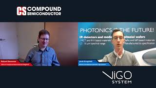
Multimodal Spectroscopic Characterization of Large Semiconductor Wafers
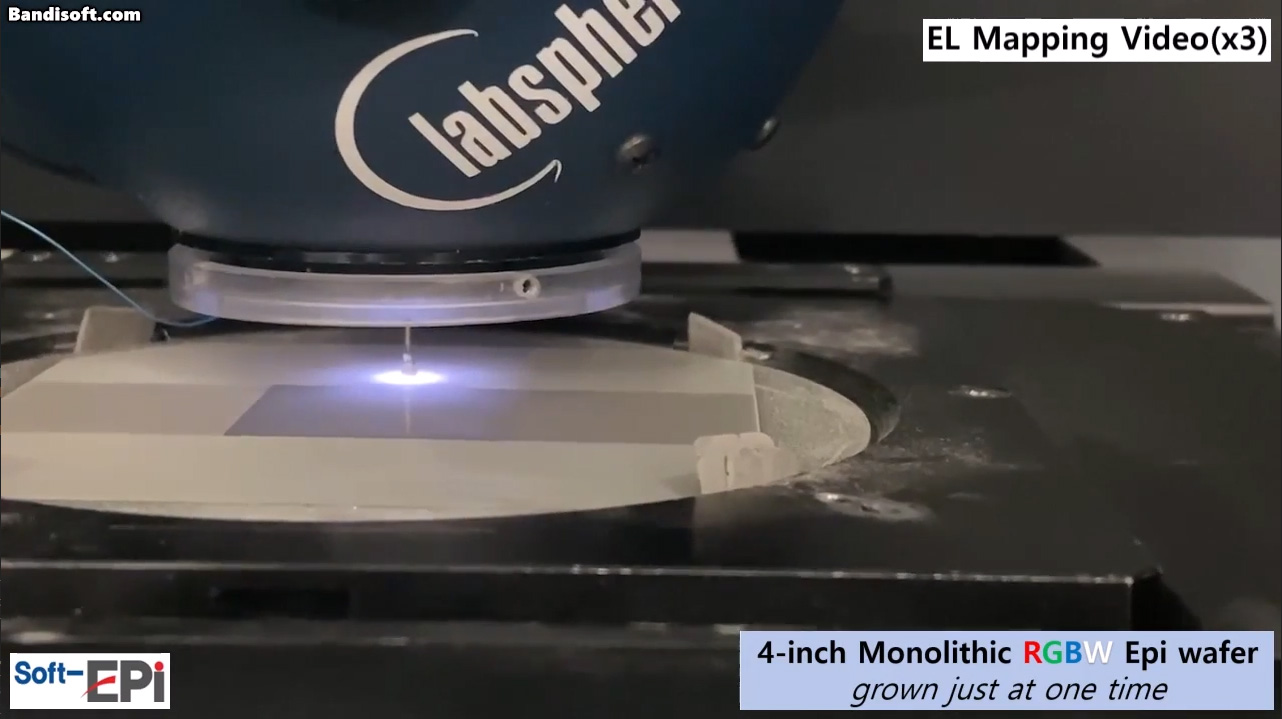
Video Summary
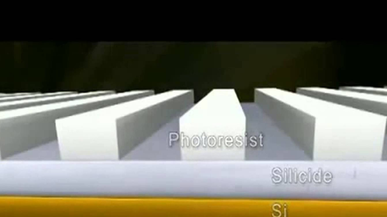
The simultaneous need to increase performance and reduce cost for today's semiconductor devices means using ever larger wafers, while reducing the size of device structures, thereby increasing their complexity. This combination of requirements means the metrology tools for characterizing such wafers need to evolve to handle such large wafers – up to 300mm in diameter. At the same time, these tools need to increase in sophistication to unravel the complexity in the ever-smaller device structures.


![Nel Hydrogen - On-Site Hydrogen Production - Webinar [Chinese version]](https://cdn.bitmagazine.net/assets/images/videos/0_webinar_nelhydrogenChinese.jpg)