AFRL develops Gallium oxide capability
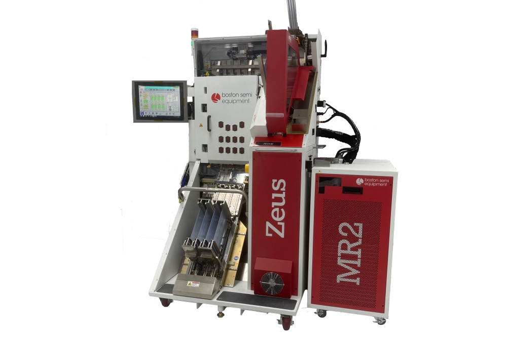
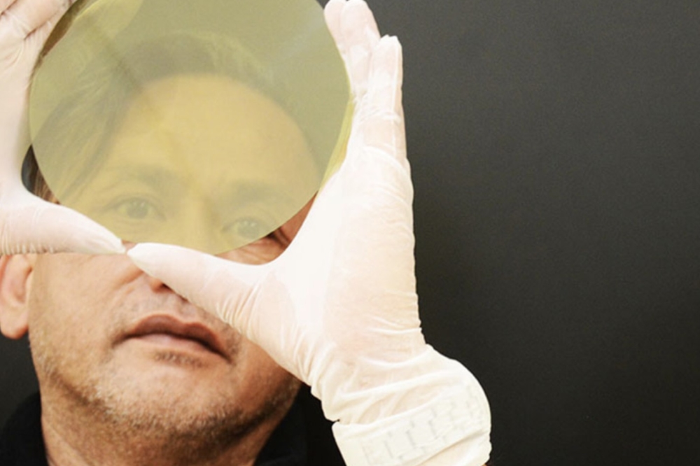
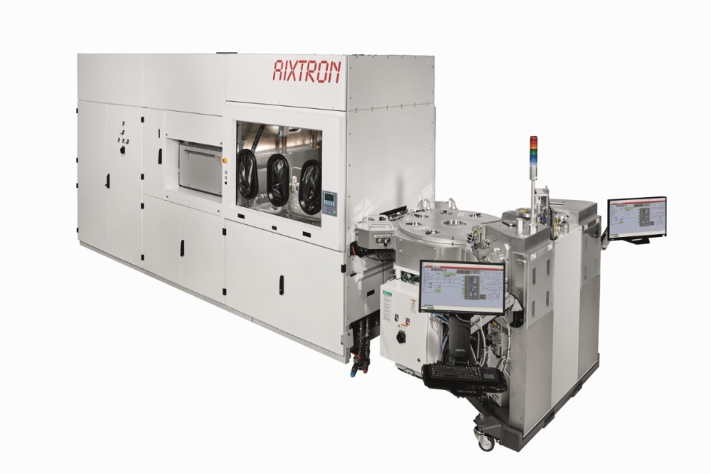
Shin Mou shows off the laboratory’s new MBE chamber
The US Air Force Research Laboratory (AFRL) in Ohio, has announced an emerging capability for growing gallium oxide semiconductors. The new Oxide MBE laboratory is said to be a first-of-its-kind capability within the US.
“This is the first system of this kind specifically designed to grow gallium oxide, which is a promising new material for high-performance electronics,” said Materials research engineer Don Dorsey.
Dorsey explains that while gallium oxide is not a new material, its recent discovery as an emerging electronic material means much remains to be learned about its properties and performance. Unlike commonly-used silicon-based semiconductors, gallium oxide can handle much higher operating voltages. As a result, it can be used very effectively for high-power, high-voltage applications.
What this means for aircraft electronics is that current components that are necessarily big and bulky could be made much smaller and lighter. Dorsey likens this to today’s common laptop voltage converters.
“A simple example is the power adaptor located on the cords of laptop computers. We think the promise of this is that you could get rid of that entirely and have a small component on the circuit board that would do the same job.” Dorsey explained that the AFRL team’s work is geared toward similarly reducing the weight and size of Air Force systems.
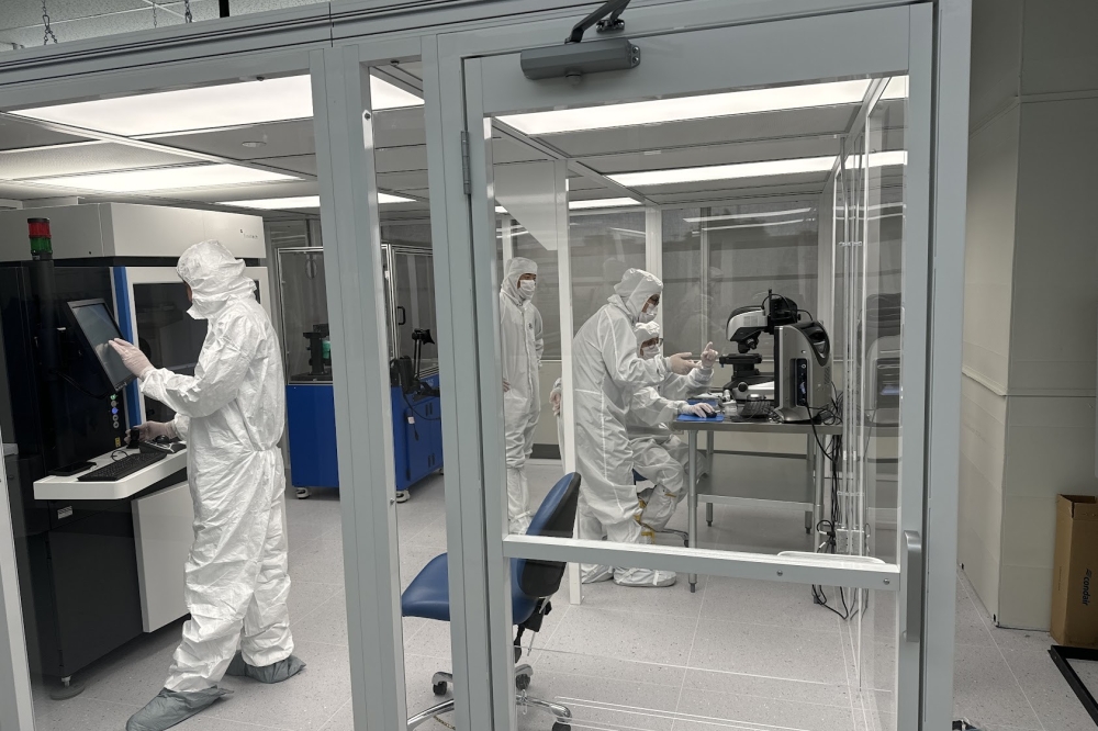
What makes AFRL’s Oxide MBE Laboratory ideal for this this type of materials research is that it is specifically and solely designed for the growth of gallium oxide. As Dorsey explained, contamination is a critical factor in the growth of quality crystals. Since the new MBE chamber will only be used for gallium oxide, there is no chance of cross-contamination that could degrade the material quality.
“This unique piece of equipment gives us an advantage,” said Dorsey. “We are able to produce extremely pure samples and have the assurance that our material formulations are exactly as we intend them.”
The MBE capability enables AFRL materials experts not only to produce high-quality semiconducting materials, but to further refine their production capabilities through a synergistic relationship with AFRL sensors researchers, who incorporate the materials into their electronic components. The sensors experts then provide feedback to the materials team, who use that information to adjust the material growth in the MBE chamber. This back-and-forth process is helping the team to learn more about the formulations that produce the best quality semiconductors for application-specific purposes.
According to AFRL materials researcher Shin Mou, the MBE Laboratory also equips AFRL to bridge the gap between university and industry research efforts. “The capability to produce up to four-inch wafers enables us to work with university Centres of Excellence as well as industrial research organisations to advance the material capabilities and open new doors for this technology.” He explained that AFRL will be able to pull from the research conducted within academia, put the fundamental understanding into action to further develop wafer-scale materials, and transfer the knowledge to industrial partners for commercialisation.
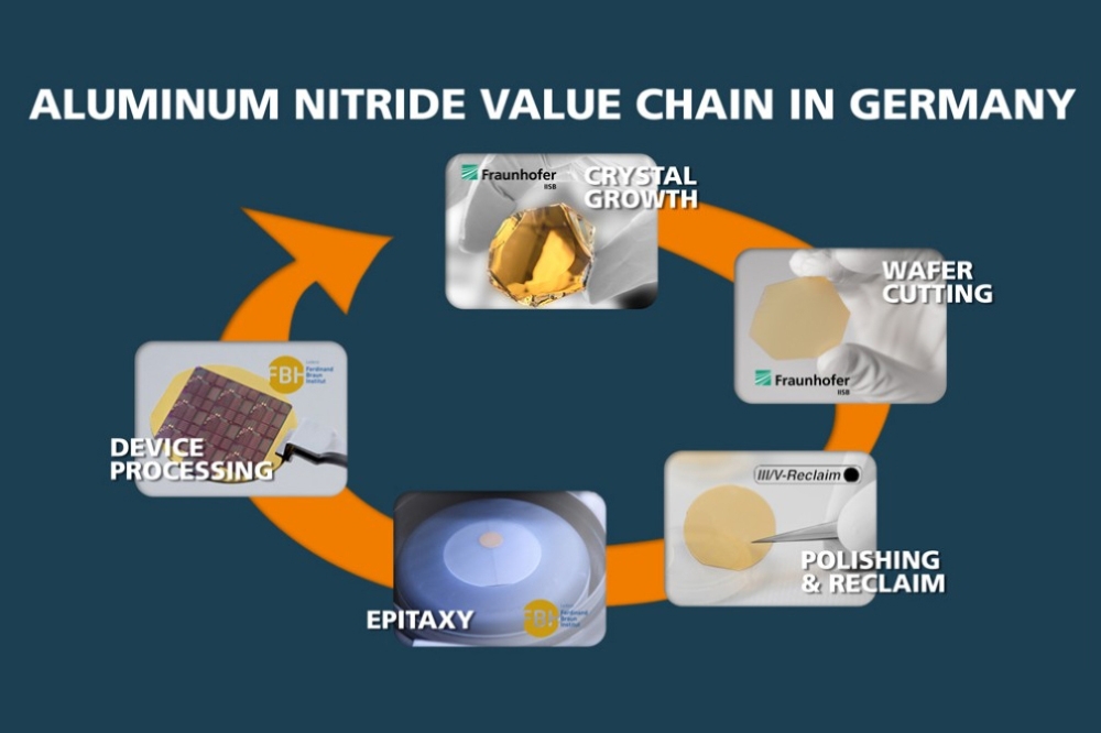
Mou explained that the long term goals for this work include refining the material to the point that it can be transferred to U.S. industry for large-scale production. Having a domestic supply chain for advanced semiconductors would ensure widespread, low-cost availability of these materials for both military and commercial use.
An important immediate step for the AFRL research team was the recent opening of the AFRL-Cornell Centre for Epitaxial SolutionS, or ACCESS. This Center of Excellence, led by Cornell University in partnership with AFRL, will give Cornell students and faculty the opportunity to work closely with AFRL researchers and laboratories. The knowledge base that grows out of ACCESS will go hand-in-hand with the ongoing AFRL efforts including the MBE research, resulting in a greater breadth of knowledge and expertise.
“We are excited about this collaboration with the university community,” said Air Force Office of Scientific Research Program Officer, Ali Sayir. “The Centres of Excellence provide a means by which we can facilitate and draw from student and faculty research, while at the same time introduce students to the AFRL community and potential professional opportunities within. This centre is aligned well with the AFOSR mission and investment strategy on ultra-wide band gap materials funded through AFOSR core grants and Office of the Secretary of Defense investment on several Multi-Disciplinary University Research Initiatives.”
“This is a very exciting time in the evolution of this technology,” said Dorsey of the new MBE lab and university partnership. “These are major enablers for the advancement of these capabilities. The work we’re doing will be a major step toward a new breed of high-power electronics to better enable the warfighter for tomorrow’s challenges.”


