Project to develop EV-grade 1.2 kV SiC MOSFETs

Oxford Instruments will be working with Hitachi Energy Switzerland and the University of Warwick to improve SiC power MOSFET gate technology through the use of ALD oxides.
This is one of 26 new projects intended to enhance UK and Swiss collaboration on innovation and technology, supported by £7.8 million funding from Innovate UK and similar figure from Innosuisse, the Swiss innovation agency.
Hitachi Energy Switzerland (Hitachi) has a proven track record of developing automotive grade SiC power MOSFETs with a reputation for products with novel MOS interfaces.
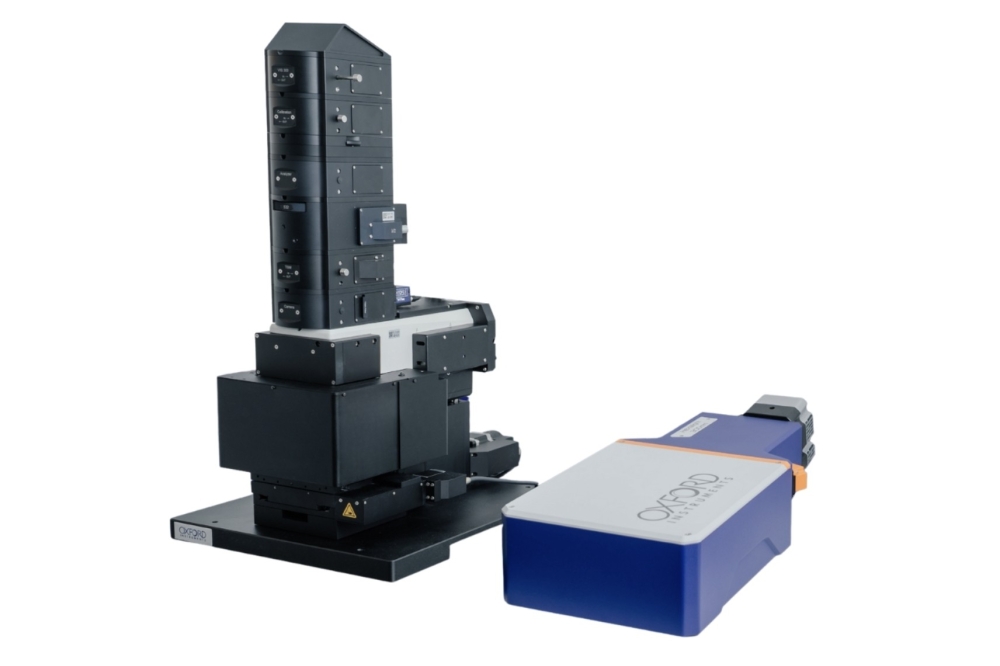
Oxford Instruments Plasma Technology (OIPT) has developed a novel oxide deposition process that uses a remote plasma source in a commercial atomic layer deposition (ALD) system. This process is suitable for the formation of gate oxides in wide bandgap semiconductors.
A research team at the University of Warwick (UoW) has recently developed an ALD SiO2 deposition process on SiC that has the potential to be commercialised.
This project will bring together the three groups and their relative expertise to demonstrate the potential of ALD oxides in the formation of EV-grade 1.2 kV SiC MOSFETs.
The aim is address one of the most pressing issues in the adaptation of this technique by fundamentally changing the way of forming a crucial part of the device, the gate oxide. Conventional dielectric and SiC interfaces are suffering from high density of defect states, hampering the further uptake of this technology.
The partners aim to deliver the first demonstration of a commercially relevant planar 1.2 kV SiC MOSFET that contains OIPT’s remote plasma ALD-deposited SiO2 and high-k dielectric (for example Al2O3) gate oxides.

