US team discovers 'hidden carrier' cooling in III-nitrides
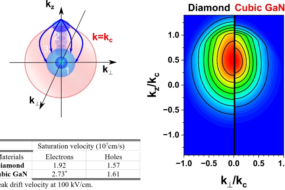
Carrier drift velocity sets the ultimate speed limit in a semiconductors has been studied in-depth. In power electronics applications where the electric field is high, the saturation (or peak) velocity becomes the limiting factor in how much current one can conduct.
Empirical equations for saturation velocity are available, and reportedly governed only by (1) conductivity effective mass and (2) optical phonon energy. Now, recent work by the University of Illinois Urbana-Champaign is offering an alternative perspective.
In IEEE Transactions on Electron Devices, Jaekwon Lee, Can Bayram, and Jean-Pierre Leburton disclose a new 'hidden' parameter: the nature of high-energy phonon scattering, affecting the saturation (or peak) velocity.
The team compares the high-field transport properties of cubic GaN and diamond, governed by different scattering mechanism: Randomizing optical deformation potential (ODP) scattering in diamond vs. non-randomizing (i.e., forward-preferring) polar optic phonon (POP) scattering in cubic GaN.
The results reveal that non-randomizing POP scattering in cubic GaN results in 'carrier cooling', leading to higher peak drift velocity than what is thought it should have. This means carriers are less 'spread' or more of the carriers are 'focused' to the field direction in cubic GaN. Their finding explains why cubic III-nitrides can have higher peak drift velocity than what is thought possible and advocates cubic GaN, AlN and BN as a potential high-saturation-velocity materials for power electronics.
Pictured above: (left) Simplified scattering model for drift velocity calculation and tabulated carrier saturation velocities; and (right) The comparison of electron distribution function of diamond and cubic GaN at 20 kV/cm.
Reference
'High Field Transport in (Ultra) Wide Bandgap Semiconductors: Diamond vs. Cubic GaN' by J. Lee, C. Bayram, and J.-P. Leburton; IEEE Trans. Electron Devices (2024)

