Halo closes $80M funding round

Halo Industries, a Stanford University spin-out, has raised up to $80 million to help establish what it describes as a 'new gold-standard' of SiC substrate production.
The oversubscribed Series B funding round was led by Thomas Tull’s US Innovative Technology Fund (USIT) with participation from 8VC and SAIC.
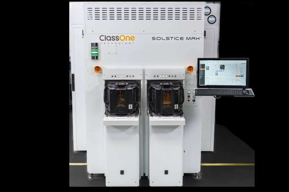
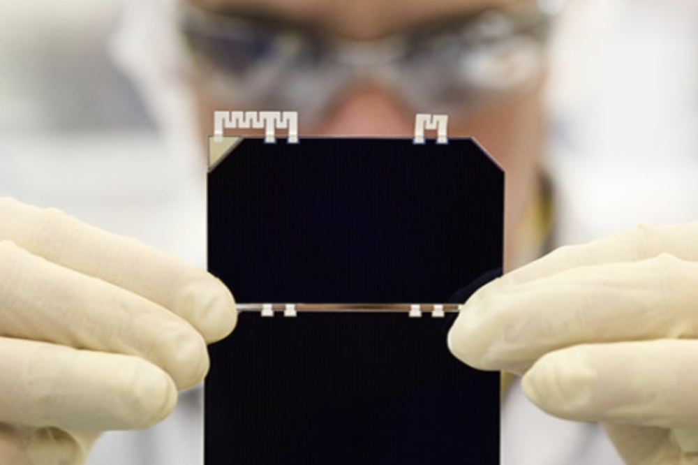
Halo Industries manufactures several materials used for semiconductor production, including SiC wafers. SiC is a hard, brittle material that is challenging to cut. Halo's proprietary laser-based slicing tools are designed to increase yield and quality of SiC while minimising waste and production cost.
The company's laser manufacturing technologies have also been demonstrated to work on silicon, diamond, sapphire, lithium tantalate, GaN, and others.
“Amid the explosive growth in demand for next-generation power electronics with improved energy efficiency, our laser-based manufacturing tools and SiC production are critical components for maintaining momentum in clean tech development,” said Andrei Iancu, Halo Industries founder and CEO. “This financing will serve as the foundation for our future strategic engagements where our innovations can reshape market economics as well as enable entirely new device architectures and functionalities.”
Peter Tague, managing partner of USIT said: “Halo Industries allows US companies to onshore manufacturing by competing on innovation, efficiency and cost, creating a durable advantage that is additive to recent industrial policies and eases supply chain challenges. We see a bright future for Halo Industries to foster innovation across industries and diverse applications, from renewable energy and electric vehicles to telecommunications, grid infrastructure, and defense customer bases.”

