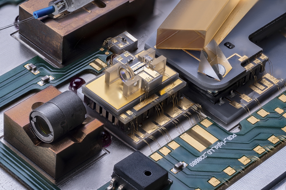
Nexperia ramps SiC and GaN with Aixtron tools
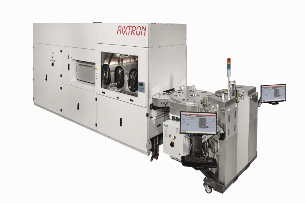
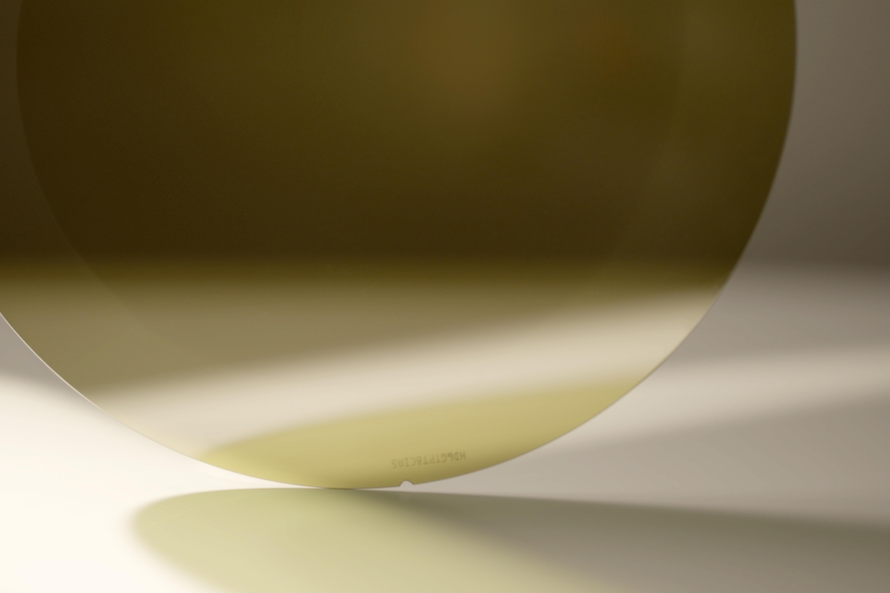
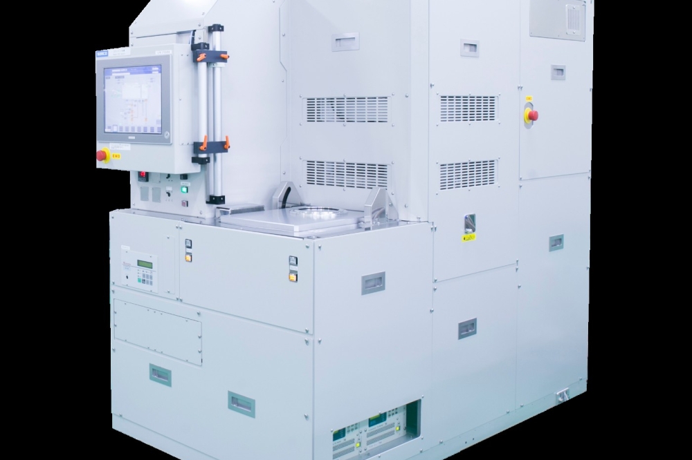
Aixtron has announced it is supporting Nexperia's ramp-up of 200mm volume SiC and GaN power device production. With the new G10-SiC for the 200mm SiC volume ramp, Nexperia is placing a repeat order for Aixtron SiC tools, and an order for Aixtron G10-GaN tools.
Nexperia, headquartered in Nijmegen (Netherlands), operates front-end factories in Hamburg (Germany) and Greater Manchester (England). The Aixtron epitaxy systems will be installed at Nexperia’s wafer fab in Hamburg (Germany). Nexperia’s Hamburg site produces approximately 100 billion discrete semiconductors annually, accounting for about a quarter of the global production of this type of products.
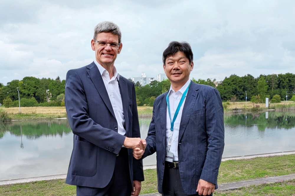
“We are honoured to strengthen our alliance with Nexperia, a pivotal player in the semiconductor landscape. Our G10 epitaxy solutions are at the heart of this collaboration, bolstering Nexperia’s growth strategies and enabling the high-volume production of wide bandgap semiconductors for commercial applications. Together, we are setting the pace for the industry’s transition to more energy-efficient SiC and GaN solutions”, said Felix Grawert, CEO and President of Aixtron SE.
“As we advance our technological capabilities and market presence in high-power semiconductor production, our strategic partnership with Aixtron is transformative. Integrating the G10 systems will significantly enhance our wide bandgap technology development and production capabilities. We build on Aixtron's proven uniformity and leverage the additional productivity gains of Aixtron’s G10 tools to scale up our production efficiently and cost-effectively. With the new G10 tools in our Hamburg facility, we are poised for further advancements in our production capabilities,” said Achim Kempe, COO at Nexperia B.V.