Qromis recognised by Frost & Sullivan award

Frost & Sullivan recently researched the GaN semiconductors industry and, based on its findings, has recognised Qromis with the 2024 Global Enabling Technology Leadership Award.
"Qromis is building on its early commercialisation success by consistently demonstrating efforts to innovate, create, and focus on diverse applications, accelerating GaN penetration in the power, RF, and microLED markets. Consequently, the company is well-positioned to experience continued growth above that of the GaN devices market," said Prabhu Karunakaran, industry principal for the semiconductors program at Frost & Sullivan.
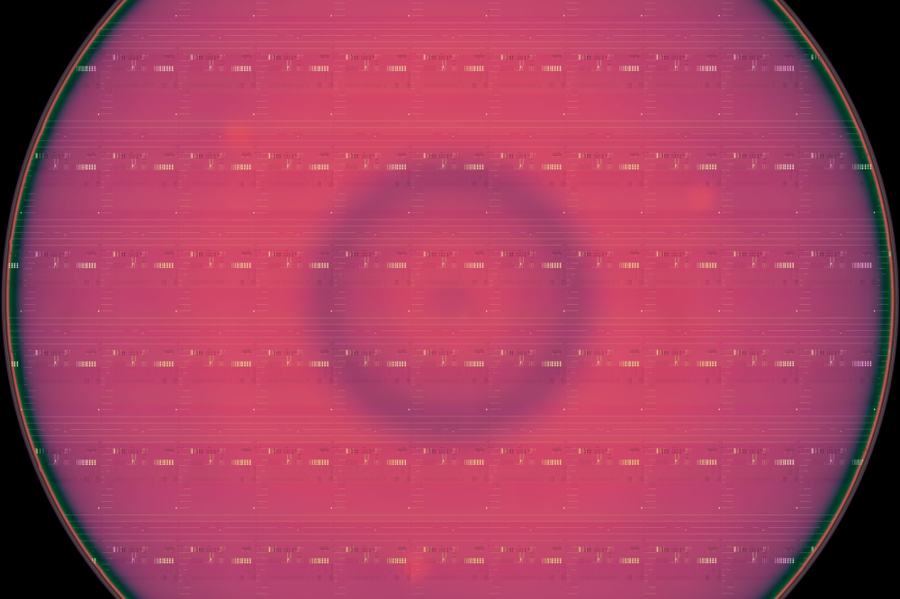
Qromis has a patented CMOS fab-friendly substrate called QST for GaN devices, which reduces costs and increases the reliability. QST technology has an embedded high thermal conductivity and high mechanical strength core material which has a very closely matched coefficient of thermal expansion to those of GaN/AlGaN epitaxial layers over a wide temperature range.
These features enable high performance GaN power device manufacturing on 200 mm and 300 mm mainstream CMOS production platforms. This applies to mainstream lateral GaN power devices and also vertical GaN power switches and rectifiers suitable for high voltage and high current applications presently dominated by Si IGBTs and SiC power FETs and diodes.
In addition to GaN power electronics, the technology is suitable for GaN RF and microLED applications.
One of the critical features of QST technology, says Frost & Sullivan, is the robust wafer shape control, epitaxy uniformity and elimination of costly and complex strain management layers which result in reduction of epitaxy growth time by 50 percent. This is an important and leap-forward achievement for overall cost reduction of GaN devices.

