Axus announces strong sales momentum for CMP tool
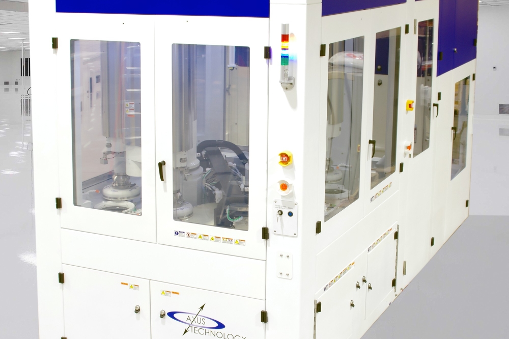
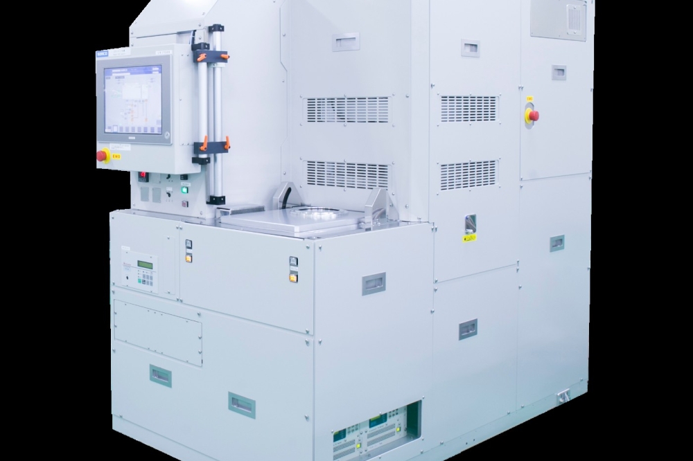
Axus Technology, a provider of chemical mechanical planarisation (CMP) equipment, has announced strong sales momentum for its Capstone CS200 CMP processing tool.
In recent months, the company has received orders from SiC semiconductor makers based in Europe, Asia and North America.
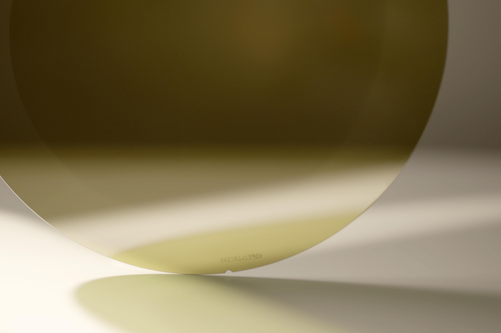
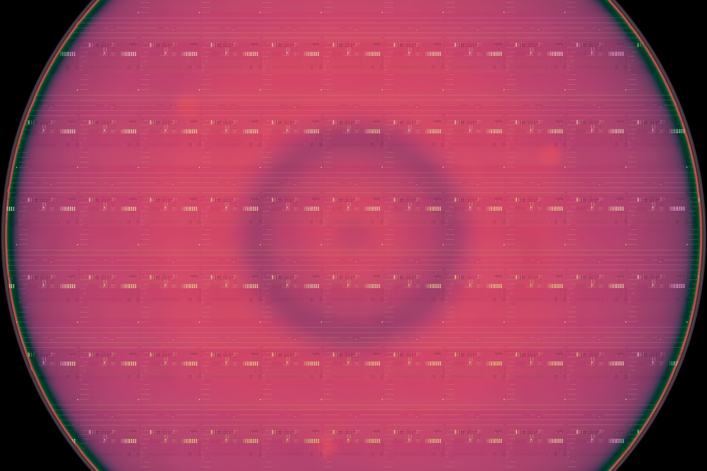
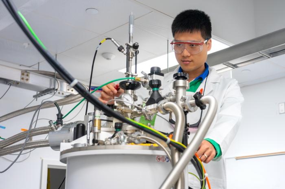
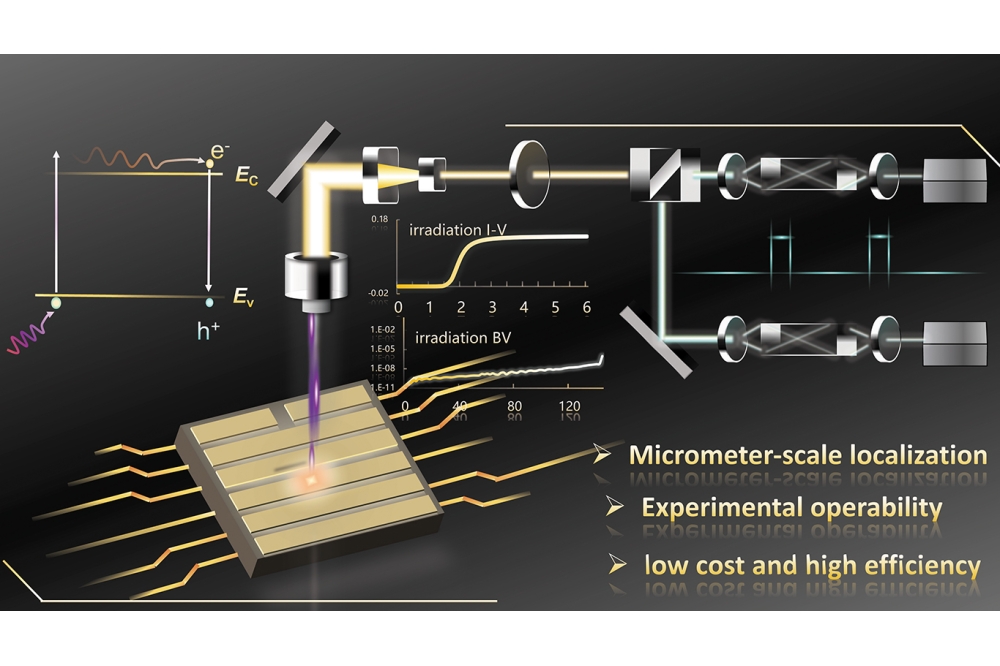
The Capstone orders include R&D/engineering and production-ready tools, with the latter configured for volume production of both 150mm and 200mm wafers. Capstone can process two different wafer sizes simultaneously, enabling the tool to deliver industry-high throughput and yields.
“Many of our customers represent the top tier of SiC device and/or wafer manufacturers worldwide,” explained Catherine Bullock, Axus Technology’s director of process technology. “These customers have conducted extensive process and equipment testing to thoroughly characterise and compare various solutions for advanced SiC CMP. I’m proud to say that all of them selected Capstone as their preferred platform. This is particularly relevant given the significant challenges and differentiation associated with CMP for SiC as compared to more mature CMP applications.”
“This is an exciting time in our industry,” said Axus Technology CEO Dan Trojan. “SiC is growing at a rapid pace – much faster than CMOS – fueled by demand for power electronics applications such as AI data centres, renewable energy and EVs. With our SiC engineering brain trust, proven product portfolio in CMP and related technologies, and growing base of leading suppliers and SiC customers – evidenced by this recent order influx – Axus Technology is well positioned to become the industry leader in CMP for compound semiconductors.”
Axus says it is consulting with developers of SiC and other compound semiconductor devices to help them determine their optimal path for scaling from 150mm to 200mm production. With its recent infusion of capital funding, the company is stepping up its focus on scaling to HVM, enabling the company.