Ammonia MBE targets HEMTs that feature ScAlN
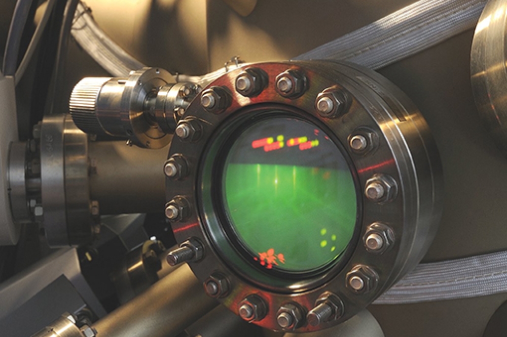
Enhancing GaN-based HEMTs with ScAlN, via growth by ammonia MBE, promises to improve the performance of high-frequency power devices.
BY YVON CORDIER FROM UNIVERSITÉ CÔTE D’AZUR, CNRS-CRHEA
Within our community, much effort is devoted to developing new material systems with the potential to produce higher-performing devices. Often this work involves much breaking of new ground, but sometimes it’s possible to get a helping hand by considering materials that have already enjoyed success in related fields.
For many years, one of our significant revenue streams has been the GaAs-based PA, which plays a key role in the RF front-end of billions of handsets. Sitting close to the PA is another crucial component in this part of the mobile, the acoustic-wave filter. It faces demands that have become far more strenuous over the years, and since 2009 there has been much interest in meeting these more stringent requirements by turning to the alloy scandium aluminium nitride (ScAlN). This relatively novel material is an attractive alternative to the incumbent, AlN, offering a larger response, realised when adding scandium with a mole fraction of about 20 percent to 40 percent to the original AlN.
Figure 1. Schematic cross-section of the first (left) and second (right) generation HEMTs studied at CRHEA.
Recently, due to its wide bandgap characteristic, ScAlN has started to gain attention as an attractive candidate for fabricating electron devices, with this ternary promising to play a key role in GaN-based heterostructures. This interest tends to focus on the HEMT, a very popular high-frequency electron device that can be based on the nitride family of materials.
Compared with a compound semiconductor like GaAs, GaN presents several advantages when fabricating a HEMT. As well as a critical electric field that is ten times larger – and provides a commensurate increase in breakdown voltage – GaN features a wurtzite crystal lattice that spawns internal electrical polarisation, leading to electrical charge, either at the surface, or at the interface between this material and other compounds. Thanks to this doping-free charge, free electron densities as high as 1 x 1013 cm-2 are realised at the interface of alloys like GaN and AlGaN – that’s more than five times that found in a typical AlGaAs/InGaAs pseudomorphic HEMT.
Another strength of the established nitrides is that when AlN is grown on GaN, this leads to the generation of up to 5 x 10¹³ electrons per cm². However, there is a downside of this pairing: a difference in the natural distance between aluminium and nitrogen atoms, compared with that for gallium and nitrogen. This mismatch induces considerable mechanical stress inside the crystal lattice, hampering the fabrication of stable materials and devices.
Due to this issue, there is much interest in alternative alloys, such as InAlN and ScAlN. For both these ternaries, there is almost no stress when they are grown on GaN, when the aluminium mole fraction is around 85 percent.
While much effort has been devoted to InAlN, ScAlN is the more promising of the two. In terms of electron density, ScAlN can reach a value of around 4 x 1013 cm-2 in the GaN channel, about twice that of InAlN. A high value is cherished, as this helps maintain a carrier density of more than 1013 electrons per cm², even for film thicknesses between 5 nm and 10 nm. This strength is analogous to that of oxide thinning in a silicon MOSFET, an approach employed to limit the short channel effect – this is the undesirable weakening of drain-current modulation with gate bias, occurring when shrinking the gate to 100 nm or less to cut the carrier transit time and reach operating frequencies of several gigahertz or more.
Note that unlike InAlN, ScAlN can be ferroelectric. This asset offers opportunities associated with memory, and also for programming the threshold voltage of transistors.
Figure 2. High resolution X-ray diffraction performed on a ScAlN film grown by ammonia MBE on a GaN.
The need for epitaxy
For the fabrication of filters operating at a few gigahertz, sputtering can deposit ScAlN with sufficient chemical and structural quality. But this form of film growth is not capable of producing a stack of semiconductors with sufficient crystal quality and purity for making HEMTs with high performance. For this reason, heterostructures are epitaxially grown on monocrystalline substrates, such as sapphire, silicon or SiC (see Figure 1).
Within the family of epitaxial growth techniques, plasma-assisted MBE produced the first ScAlN epilayers. This form of epitaxy involves the evaporation of pure metal atoms under high vacuum. As nitrogen molecules are very stable, this gas is introduced in the growth chamber through an RF cavity, employed to generate radicals that combine with metals to form III-nitride compounds. The constituents come together on the surface of a substrate, radiatively heated by a resistive filament positioned close to the back face.
Like all epitaxial techniques, certain conditions are essential for high-quality material growth. They include the growth temperature, which has an operating range that is governed by the conditions for generating nitrogen radicals and their reaction rate with metals. Optimum conditions for growth of GaN rely on a subtle equilibrium between the metal reaction with nitrogen, and metal re-evaporation at a temperature around 700 °C, resulting in the accumulation of a gallium layer floating on the surface. It’s not easy to realise this state of affairs, as a slightly lower temperature leads to the accumulation of metal droplets at the surface, and
a higher one generates defects due to a lack of metal. It’s even more challenging to grow high-quality layers of ternary materials, because different metals react with nitrogen radicals at different rates, and re-evaporate at different rates. But despite these complications, plasma-assisted MBE is the most common epitaxial technique for growing ScAlN-based heterostructures.
For nitrides in general, MOCVD is the most widely adopted approach to growth. But it’s held back by a lack of scandium-containing organometallic precursors with sufficient partial pressure. While new precursors are looking to address this issue, even if there is success on this front, there’s still the challenge of fabricating heterostructures with sharp interfaces at the high temperatures necessary for good crystal quality and high-purity material. In this context, ammonia-source MBE has much promise, allowing GaN growth at temperatures around 800 °C under an excess of nitrogen, a condition that guarantees easy control of growth rate and material quality.
Figure 3. Capacitance-voltage and corresponding charge density in the 2DEG of a ScAlN/GaN HEMT grown by ammonia MBE.
Using this epitaxial technology, our team at CRHEA, France, has been developing and refining ammonia MBE since the 1990s. With this approach we draw a parallel to MOCVD, thermally cracking ammonia at the surface of the heated substrate. In our case the temperature is sufficiently low to limit diffusion in the crystal, but high enough to ensure growth of smooth films with a relatively high purity. Additional assets are that: ammonia consumption is far lower than it is with MOCVD; the undoped GaN that’s produced by this technique is sufficiently resistive to enable the fabrication of functional transistors on HEMT heterostructures; and the control of the growth of alloys, such as AlGaN, is facilitated by the fact that all the gallium and aluminium atoms reaching the surface can be incorporated into the crystal.
Since the beginning of this century, our laboratory has been using ammonia MBE to produce AlGaN/GaN HEMTs on silicon substrates for RF power applications. By working with partners that include IEMN, ETH Zürich, Daimler Chrysler, Thales, and the III-V Lab, we have realised CW power densities of 6.6 W mm-1 at 2 GHz and 3.2 W mm-1 at 40 GHz with our material.
We started investigating the growth of ScAlN in 2021. Back then, in terms of scandium-containing alloys, only ScGaN had been grown by ammonia MBE. We began by focusing on the effect of the growth temperature, supported by funding from the French ‘Investments in the future’ programme named GaNeX and the European ECSEL JU project Gallium Nitride for Advanced Power Applications (GaN4AP).
This study determined an optimal growth temperature window of around 670 °C, and demonstrated that it’s possible to grow films on GaN with low strain that have a scandium molar fraction of around 14 percent. For this work, our collaborators studied film quality at the GREMAN laboratory in Tours, GPM in Rouen, France, and CNR-IMM in Catania, Italy – and we benefited from fruitful discussions with Fraunhofer IAF in Freiburg, Germany. Characterisation rapidly revealed the advantages of ammonia MBE for ScAlN alloy growth, determining that there is no change in scandium content throughout a widely explored 180 °C growth temperature range, and it’s possible to grow uniform random alloys free from metallic precipitates, like Al3Sc, which can plague plasma-assisted MBE.
We confirmed the high crystal quality of the ScAlN films grown on GaN-on-sapphire with X-ray diffraction (see Figure 2). Interference fringes in the diffraction spectrum highlight low roughness for both the surface of the ScAlN film and its interface with GaN.
To rapidly assess the number of charges that are present in our HEMT’s two-dimensional electron gas (2DEG) that’s formed in the GaN channel and at the interface with ScAlN, we have used the mercury probe capacitance-voltage technique. This has determined high carrier concentrations, in the range 3-4 x 1013 cm-2 in HEMT heterostructures with an ScAlN barrier that’s around just 10 nm thick. That’s a very encouraging result for high-frequency applications.
As our HEMTs are grown on a highly resistive buffer and substrate, we are able to determine their transport properties with a contactless technique involving Eddy currents (see Figure 4). In the plots of these results, the dashed lines represent calculations corresponding to different values for electron mobility. In addition, there’s data from Hall-effect measurements, obtained using Van der Paw cloverleaf patterns fabricated on some of these samples. Note that almost all the data is bounded by two lines, corresponding to electron mobilities of 500 cm² V-1 s-1 and 1000 cm² V-1 s-1.
The single result sitting outside this domain is for a HEMT grown without an AlN interlayer that exhibits a higher sheet resistance, due to a reduced electron mobility. This observation underlines the critical role of the thin AlN (1-2 nm) layer in obtaining sharp interfaces with an energy barrier that confines the 2DEG in the high-electron-mobility region provided by the GaN channel, while not suffering from scattering associated with ScAlN.
Figure 4. Transport properties of the 2DEG in a ScAlN-based HEMT grown by ammonia MBE.
Critical capping layers
Using this first-generation material, we have fabricated transistors with a low gate leakage, and with a drain current capability of 2-3 A mm-1. However, we have found a lack of stability during device processing. We attribute this to the susceptibility of scandium to oxidation, which is a significant downside of working with ScAlN. We find that when the surface of this alloy is exposed to air, a 2-3 nm thick oxide layer spontaneously forms. What’s more, when immersed into a photoresist developer etching occurs, progressively reducing film thickness at each lithographic step of device processing.
To tackle this issue, we are introducing capping, using thin layers of AlN and GaN, grown immediately after ScAlN. According to data shown in Figure 4, capping layers don’t impede 2DEG transport properties. In a HEMT that has a total thickness for the barrier and the cap layer of less than 10 nm, the sheet resistance is as low as 210 ohm/sq. Thanks to these advances, more stable device processing has been undertaken by our colleagues at IEMN in Lille, France, enabling short-gate transistorswith a maximum oscillation frequency over 100 GHz, based on a ScAlN/GaN HEMT on a silicon substrate.
Characterisation of these HEMTs, featuring a 75 nm gate, reveals a 2DEG carrier density of 1.6 x 1013 cm-2 and a mobility of 621 cm² V-1 s-1. Evaluations of DC performance have revealed a drain current density of 1.35 A mm-1 and a transconductance of 284 mS mm-1, and an assessment of RF performance has determined a cut-off frequency of 82 GHz, and a maximum power gain frequency of 112 GHz, indicating that these devices are promising candidates for serving in the Ka band.
Next steps
Our efforts have provided the first demonstration of using ammonia MBE for fabricating high-frequency HEMTs. Building on this foundation, ScAlN/GaN heterostructures could be used for power-switching transistors, which could benefit from a low 2DEG sheet resistance, so long as we realise efficient surface passivation and preserve low leakage currents. Working towards this goal, we are investigating passivation with in-situ SiN, drawing on a process we previously developed for AlGaN/GaN-based heterostructures.
Another avenue for further work is the use of epitaxy for growing our material systems on other semiconductor films or substrates. This approach could allow us to more fully explore various functionalities provided by the piezoelectric and ferroelectric properties of ScAlN, and more generally ScAlGaN compounds. As part of such efforts, in the national project TWINS, we are developing a monolithic, voltage-controlled oscillator operating in the 1-10 GHz range, based on joint use of SAW devices and transistors. We are also involved in another national project, named BE-SAFE, that’s dedicated to the study of ferroelectric properties.
As we pursue the targets of these projects, this may generate numerous questions concerning the relationship between properties, reliability, crystal quality, and the purity of different co-integrated materials. What is for sure is that we have some exciting years ahead of us, exploring a field that’s new and wide.


