
Swansea’s superpower: The Centre for Integrative Semiconductor Materials
Buoyed by the emergence of Vishay Intertechnology within the South Wales compound semiconductor cluster, Swansea University’s recently constructed Centre for Integrative Semiconductor Materials (CISM) is focusing on power electronics while encompassing a broader portfolio of activities that includes CdTe solar cells and molecular electronics.
RICHARD STEVENSON INTERVIEWS CISM’S OWEN GUY, MIKE JENNINGS AND DAN LAMB
RS: In 2023, you opened the Centre for Integrative Semiconductor Materials. What does this choice of name reflect? And in particular, what’s meant by integrative?
OG: The concept of CSIM is to explore and develop multiple materials and technology sets. In particular, we are looking at silicon carbide, gallium oxide, gallium nitride and some of the newer thin-film technologies, which might be known as organic semiconductors.
The integrative aspect is to potentially integrate or hybridise some of those technologies.
I think the integrative name also applies to the integrative nature of what we do here in the cluster, very much supporting each other, including our industry partners. That’s in terms of technologies, research and development of processes, and also in terms of the education and skills landscape.
RS: Where did the idea for this marvellous purpose-built fab come from? And who are the trailblazers?
OG: It really stemmed from Paul Meredith coming back to Wales. He was out in Australia for many years, but he came back to Swansea, and then the initiative for CISM really started in earnest. There’d been a lot of activity in semiconductors previously, but Paul galvanised that.
This activity coincided with Wyn Meredith, Paul’s brother, coming back to Wales from Scotland. They had the vision of forming this centre at Swansea.
SPTS, now KLA, and Microchip, and the Newport Wafer Fab that’s now Vishay, had historically collaborated very closely with Swansea on various projects. CISM takes that to the next level.

The boardroom at CSIM includes a portrait of Ken Board, an emeritus
professor at Swansea University in the department of electrical and
electronic engineering. After graduating at Swansea in 1964, Board held a
research post with Philips Research labs in Redhill, before taking an
academic position at Swansea University as a lecturer, researching
semiconductor devices and their technologies. As well as Ken Board and
his family, those pictured in the boardroom include Swansea academic’s
Mike Jennings, Owen Guy, Paul Meredith, and Mohammed Darwish from
Vishay.
RS: Prior to the launch of CISM, what were the semiconductor-related efforts that took place at Swansea University?
OG: They go back many, many years. Ken Board, who our boardroom is named after and includes his portrait, is historically a big name in the field; and Mike Jennings and I were involved in work on silicon carbide 20 years ago as part of Phil Mawby’s group, Phil is now at Warwick. There’s also surface science activity at Swansea, and work on metal semiconductor contacts stemming back to Robin Williams and Steve Wilks.
More recently I’ve worked with SPTS, now KLA, for over 20 years, and I’ve worked with the Newport Wafer Fab in some capacity for about 20 years. We’ve had very close relationships with IQE over a similar period. In fact, all those three companies were involved in a Department of Trade and Industry (now Innovate UK) project together 20 years ago.
RS: Since the launch of this centre, who are the leaders you’ve attracted and retained?
OG: Mike Jennings, who has moved from Warwick University, has had a massive influence in leading power device technology. We also brought in Dave Richie from Cambridge University. We brought in young talent like Emyrs Evans, who came from Richard Friend’s Group in Cambridge.
We’ve been quite lucky also in bringing key industry people. I’m thinking of the likes of Simon Conway, who was previously one of the key guys at Pure Wafer, which sadly closed after the fire there. Simon has been one of the key instrumental people in getting the fab running here. And Gordon Horsburgh, formerly IQE, is playing a similar role. He’s been extremely influential.
MJ: We’ve also appointed honorary academics from industry, mainly from within the cluster, such as Honorary Associate Professor, Dr Craig Fisher. We did a lot of work together on early silicon carbide rectifiers. You will frequently find him in Swansea’s CISM, giving lectures and lending us his expertise. Vishay have also kindly sponsored a number PhD students here. And Dr. Huma Ashraf in a similar capacity with KLA.
RS: Space Forge has just taken residence at CSIM. What is its thinking behind this move? And what are you offering Space Forge, and how will you benefit from this development?
OG: They get the benefit of being in the same building as experts. We get the benefit of having a thriving company in the building, and the promotion, branding and all the publicity around that, which is brilliant. I know they’re extremely supportive of CISM, and we’re extremely supportive of what they’re trying to do.

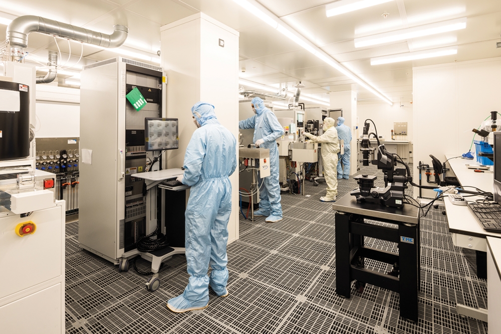
There is substantial cleanroom space within CSIM, with suite of tools
that can process epiwafers into devices, as well as extensive
characterisation equipment.
RS: Research in power electronics is a strong feature of CSIM. How much effort is being devoted to silicon carbide? And within that, what avenues are you exploring?
MJ: We’ve got the ‘Driving the electric revolution, eight-inch Silicon Carbide pilot line’. We are the open-access facility for Silicon Carbide power device development in the UK. This is wrapped into a Royal Academy of Engineering fellowship sponsored by Vishay for the purpose of using that facility to aid industry in getting their power MOSFETs into production.
We’re processing commercial wafers in this fab, right now. Much of it is simple, cleaning etc.., but there are also more advanced structures being investigated through other compatible processing, such as etching, metallisation and process module design. There’s a lead time on equipment, so we are filling as many gaps as possible for our commercial partners.
It’s also characterisation. The MOS interface in silicon carbide is problematic. Detailed characterisation requires a lot of data processing, physics equations and numerical methods. Our commercial partners send that activity to us. We’ll characterise and send the results back, etc.
We are also supporting commercial activity on another form of silicon carbide – cubic silicon carbide to be exact. I’ve got history in cubic silicon carbide, due to an €8 million EU project, which started in 2017, led by STM.
We’ve also got process development, which we’ve been doing in collaboration with KLA and also Vishay, particularly on rounded trenches, corners, and silicon carbide dicing. And the other side of KLA, on metrology and defect characterisation, because there are still lots of defects in silicon carbide, and progress to be made on that front.
I think the most exciting work we’re doing is on plasma dicing with KLA. This won best poster at ICSCRM, 2024. We’ve got a lot of interest in that for obvious reasons, improving yield and die strength. It’s not perfect yet. There’s more work to do, but that’s got real mileage.
We have a dedicated power lab for the characterisation and long-term reliability testing of packaged silicon carbide parts. We work with numerous commercial partners on the testing side. Large commercial entities obviously have their own bespoke instrumentation for this purpose, but what you find is that the large IDMs use all of their instrumentation for product. They are not set up for R&D. They don’t have the capacity, and they don’t have the flexibility either, so they come to the likes of us.
If you buy a reliability tester, it’s off the shelf. It’ll do 80 percent of the rated voltage for a thousand hours with humidity and that’s it. It’ll just tell you when its failed. But with our kit, we can programme our own voltage-ramping recipe, be very flexible with the temperature, voltage and humidity control. If requested, we can go above the rated breakdown voltage. We can do whatever test they want, within reason, and monitor the current and the failure mechanism.

Recently CSIM installed an MOCVD reactor capable of the growth of gallium oxide epilayers on 4-inch substrates.
RS: There is a lot of interest in GaN for power electronics. Do you have programmes in that area?
MJ: We work very closely with processing experts at Vishay Intertechnology on GaN. Being a power electronics guy, I want to see if GaN is limited to a maximum of three kilowatts. The main market is laptop charges, but can you get a GaN device to work at higher voltages, higher currents, higher temperatures, higher power?
We’re looking at vertical gallium nitride. When it’s lateral, when you go up in voltage, you have to make the die larger. Therefore, you have problems with yield, and it becomes commercially unviable beyond about 650 volts. We’re looking to scale up vertically, like you would a classic silicon carbide power MOSFET, and use a MOS interface. You lose some good properties, but you may be able to increase the power level.
We’re looking at HEMT technology as well. We’ve got interesting ideas on how to keep the die the same size, but increase the voltage rating.
RS: You have also commissioned a reaction for gallium oxide. Tell me about the gallium oxide efforts at CSIM.
DL: Yes, we were very fortunate to win EPSRC Strategic Equipment funding that enabled us to procure a state-of-the-art Aixtron close-coupled showerhead research reactor. The reactor can deposit a range of different semiconductor thin films, including gallium oxide and cadmium telluride. The reactor was delivered straight into a purpose designed laboratory, within CISM, and has been successfully depositing gallium oxide material since January this year. We have been providing lots of high-quality 2-inch and 4-inch gallium oxide thin films into Swansea-based research projects and the wider UK gallium oxide community.
MJ: There are a lot of challenges for gallium oxide, no question. Even with heterogeneous integration, if that’s the correct term, growing diamond or nickel oxide above gallium oxide, the p-n junction voltage is still very high. With very-high-voltage devices, like silicon thyristors, you can get over one kiloamp conduction through a device with a one-volt drop across it. You can’t even turn gallium oxide on, even with heterogeneous integration, until about three, four volts. So, how is that going to work? Our challenge is to overcome these problems, including the poor thermal properties. I was sceptical about silicon carbide as well, because I thought that its MOS channel is so poor. Turns out that one worked so who is to say that an answer will not be found for gallium oxide.

The CSIM facility is part of the Swansea Bay campus, which is home to
Engineering, the School of Management and the Computational Foundry, as
well as student accommodation with direct access to the beach. Inset:
The £50 million CISM facility on Swansea University’s Bay Campus
officially opened in 2023.
RS: You’re also involved in a project associated with cadmium telluride solar cells for powering satellites. Can you explain the role you’re playing here?
DL: 80 percent of the radiation-hard glass that protects space solar cells is made in North Wales by a company called Qioptiq Space Technology.
It’s ultrathin glass, not much thicker than a human hair, laminated on top of most space solar cells. Here at Swansea University, we had the novel idea of making cadmium telluride film solar cells directly onto the space glass. That means huge weight savings – critical for space – and even the potential for flexible solar cells that pack more efficiently. CISM has an EPSRC-funded project that is using our Aixtron close-coupled showerhead metal organic chemical vapour deposition system to make each of the semiconductor layers directly onto the ultrathin glass.
Our team is aiming for a step-change reduction in the cost of space solar cells, opening the door to emerging space power applications that require low-cost, volume manufacturing and high-radiation stability.
RS: You’re in the CS cluster. Do you think this centre would have been built were not for the cluster and the investment its generated?
OG: Definitely not. The cluster have been hugely financially supportive – and this centre was built to support the cluster. So it’s been a mutual process throughout the whole timeline.
There was co-investment from SPTS KLA, from the Newport Wafer fab, and from IQE – £15 million each over 10 years, plus additional co-investment from other industry partners. That was instrumental in helping us obtain the grant funding for this building. They’ve been extremely supportive in the technologies that we›re developing or co-developing.
RS: And how valuable is it to have a power electronics chip manufacturer within the cluster?
MJ: Having a big chip maker like Vishay on the doorstep is very, very valuable for our research. And more than that, really, our mission is to see the cluster grow and, to some extent, move on from silicon. If you’ve got a fab now, if you’re only doing silicon power chips, which is what they do in Newport, it’s going to be very, very difficult to be competitive longer term, particularly at 8-inch. So it’s great to see that they are diversifying their product portfolio, because you need to be able to turn your hand to silicon carbide, to gallium nitride.
RS: And the other partners in the cluster, like Microchip and IQE. What are the mutual benefits you’re getting there?
OG: IQE we’ve worked historically with for over 20 years. They supply materials to projects, which is hugely valuable. We’ve worked with them on solar technologies in the past.
MJ: IQE through their subsidiary company, Compound Semiconductor Centre Ltd, are developers of GaN epiwafers. It is mutually beneficial for us to prove out their material via our GaN device processes here at CISM. As you can imagine, this relationship has formed the basis of many UKRI funded projects together.
Microchip’s activity within our region is power-electronics packaging. Obviously, they’re a device manufacturer within their own rights, but their device-manufacturing activities are in the United States. We don’t have a strong packaging activity at Swansea University. We mainly focus on device fabrication technologies, and test at the die level and package level. Having a partner like Microchip is very, very important, because sometimes you do need to package chips effectively for advanced testing strategies.
RS: All clusters have strengths and weaknesses. You could argue that optoelectronics is, in relative terms, a weakness within the cluster, as there isn’t the equivalent of a Vishay to provide volume production. Do you think that in time, this would be a good thing to address?
MJ: I’m not so sure, but I’m definitely going to be biassed. The site in Newport, now Vishay, and Microchip to some extent, have worked in power management for the majority of their existence. The cluster is geared up for power technology, in my view. Furthermore, compound semiconductor power technology is an excellent entry-level activity in order to grow a commercial semiconductor cluster in the first instance. Why? It is high volume, provides plenty of jobs, has a high figure for gross value added, and only requires a 0.18 micron fab capability, unlike a quantum, memory, GPU or VLSI facility, and is therefore cheaper. Old silicon fabs and tooling can be used with little additional investment. Innovation and novelty originate from processing new wide bandgap materials at relatively lower costs compared to a 3-nanometre node at the likes of TSMC. Of course, power technologies are self-perpetuating, feeding into more-efficient power supplies and industrial drives, such as data centres and future fabs, through higher energy efficiency, helping the quest for net zero. Wide bandgap power electronic device development as a commercial activity is a no brainer, isn’t it.
I think we should focus on our strength, I think we should focus on power, as simple as that. Sensors can be integrated into the power domain, but for me, the flagship activity is wide bandgap power electronic devices.
OG: Mike’s right, the flagship activity should be power. But there is room for some other activities at a lower priority level. Within the cluster, we’ve worked on a collaborative project with IQE, CSC, and Cardiff University, developing VCSEL technology, but the majority of that project was done at Cardiff.
RS: Over the remainder of this decade, how are you expecting CISM to evolve?
OG: We’re very closely aligned with our industrial partners, and there are huge expansion plans with Vishay and KLA in particular. There will undoubtedly be a big focus on silicon carbide technology, on gallium nitride technology. A lot of that will be going into automotive, but I think expanding into other applications, such as offshore wind, and the supply chain related to that.
There’s also Paul Meredith’s activity on molecular semiconductors and films, and our work on molecular deposition technologies. These are exciting materials technologies, which can be applied to displays, thin-film solar, and probably applications we might not even have thought of.
Another area is artificial intelligence, and the integration of computer science into some of the stuff we’re doing, as a tool. That’s quite exciting.
Advanced packaging, 3D packaging, is another interesting technique for us. We might see that evolve and translate into medical sensing technologies. We are working on utilising some technologies for biosensing applications.
MJ: Having Cadence come into the region, we’ll focus on IC design. They are interested in IC design on compounds. That will help us with this more integration approach.
We run campaigns, GaN campaigns, silicon carbide campaigns. It’s not only about demonstrating the devices – this is a fab of the future. What’s a fab going to look like in the future, in order to be able to run all of these in one facility? They face these issues in fabs all over the world. If you’re a commercial fab that’s thinking about wide bandgap materials longer term, how are you going to do all this in the same fab? Imagine having to process lots of different materials, processes with one material process, potentially harming another material. It’s a whole philosophy of how you run a facility, which is really interesting.
One of the key milestones on the horizon is ICSCRM 2027, which we’ll be hosting here in the UK for the very first time, in Newport. That’s a major international conference for silicon carbide and related materials, and a real opportunity to showcase what’s happening not just at CISM but across the cluster and the wider UK. We were proud to present award-winning work at ICSCRM 2024 and bringing the global SiC and wide bandgap community here really puts South Wales on the map.


