
Passivating b-Ga₂O₃ devices
Engineers from the University of Buffalo are claiming to have realised the first successful trap passivation of b-Ga2O3 RF devices. This is accomplished by using a relatively thick layer of Al2O3, which prevents current collapse that’s detrimental to the performance of RF devices.
The team’s FETs have been formed by ‘meticulously designed’ fabrication steps that address imperfections in their predecessors.
The recent improvements will help to advance the capabilities of b-Ga2O3 RF devices, which have a high critical electric field and a good saturation velocity. Thanks to these strengths, the Johnson figure-of-merit, which provides a good yardstick for evaluating the RF potential of various materials, is higher for b-Ga2O3than SiC and GaN.
Fabrication of the University of Buffalo’s heterostructure FETs involves the etching of the Al2O3 layer and the unintentionally doped Ga2O3 layer, prior to regrowth of heavily doped Ga2O3.
Previous devices produced by the team involved a high-power reactive-ion etch before re-growth. This etch led to a high interface resistance between this layer and the two-dimensional electron gas, limiting transconductance and RF performance.
Other groups have shown that MBE annealing under vacuum can recover some of the damage caused by plasma etching, and that dialling down the power of this etch leads to very little damage, and a very low contact resistance.
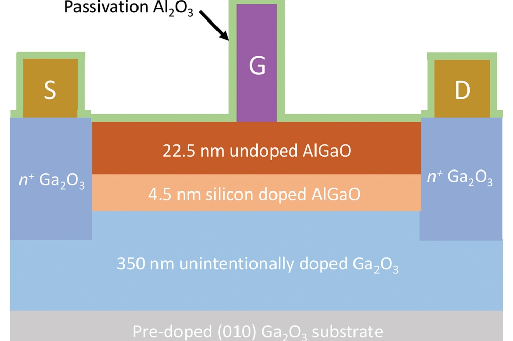
The team from the University of Buffalo have adopted both of these strategies in their latest transistors, produced by processing an epiwafer from Novel Crystal Technology, consisting of a 350 nm-thick unintentionally doped layer of MBE-grown b-Ga2O3 on a iron-doped insulating substrate.
On this platform the team added a 4.5 nm-thick layer of b-(Al0.21Ga0.79)2O3 with a silicon doping concentration of 1.5 x 1019 cm-3, followed by an un-doped barrier of 22.5 nm-thick b-(Al0.21Ga0.79)2O3.
Subsequent steps in the fabrication process included a selective low-power reactive-ion etch that ensured slow removal of the AlGaO layer and stopped on the unintentionally doped Ga2O3 layer without imparting any damage. The engineers cleaned this sample with deionised water, before loading it into an MBE chamber and annealing it at 600 °C for 1 hour under a vacuum of 10-10 Torr.
To complete device fabrication, they grew a 100 nm-thick heavily-doped n-type layer of Ga2O3, removed the growth mask, added contacts, and passivated the devices by using atomic layer deposition to form a 100 nm-thick layer of Al2O3.
Plots of drain current as a function of drain-source voltage did not uncover any non-linearity at lower voltages, an issue present in the team’s previous FETs. The team attributes the absence of this unwanted behaviour to process optimisation, including the low-power etch, the dip in hydrochloric acid prior to regrowth, and MBE annealing. Another benefit attributed to these steps is an increase in peak drain current, which hits 500 mA mm-1 at a gate-source voltage of 3 V.
Measurements also determined no significant shift in threshold voltage and no collapse in either the peak drain current or the peak transconductance after passivation, highlighting the benefit of the relatively thick layer of Al2O3.
Note that the team’s previous devices suffered from a shift in threshold voltage, which may have been caused by high-temperature deposition or plasma damage.
The team have also conducted pulsed current-voltage measurements, which revealed that Al2O3 passivates the traps and eliminates dispersion. Work by a collaboration between KBR, the Air Force Research Laboratory, Teledyne Scientific and Cornell University, have employed a similar approach and obtained moderate dispersion, but they employed an Al2O3 layer just 20 nm-thick.
RF measurements show that prior to passivation, the FETs fail to deliver any gain and suffer from huge DC-RF dispersion or current collapse.
Devices with passivation and a gate length of 191 nm have a value for the cut-off frequency (fT) of 32 GHz, at a gate-source voltage of -3 V and a drain-source voltage of 7 V. The maximum oscillation frequency (fMAX) is 55 GHz, for a gate-source voltage of -3 V and a drain-source voltage of 15 V.
Benchmarking these results, the team says that its values for fT and fMAX are amongst the highest reported for b-Ga2O3 FETs.
Pictured above: A relatively thick layer of Al2O3 passivates the traps in ß-Ga2O3 RF device
Reference
C. N. Saha et al. Appl. Phys. Express 18 071001 (2025)


