
Agnitron: Driving ultra-wide-bandgap breakthroughs
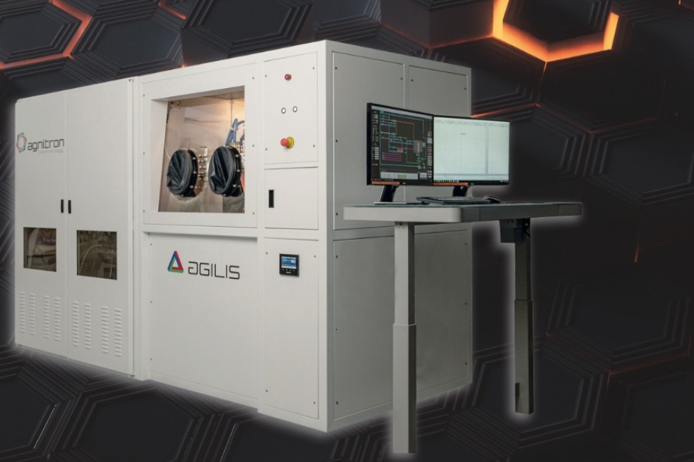
Advancing the capabilities of AlN, AlScN and aluminium-rich AlGaN is the Agnitron Agilis 100 MOCVD reactor.
BY FIKADU ALEMA, WILLIAM BRAND, BENJAMIN BRAND, AARON FINE, VITALI SOUKHOVEEV AND ANDREI OSINSKY FROM AGNITRON TECHNOLOGY
Within the family of known semiconductors, AlN possesses a number of tremendous attributes. They include a remarkably wide bandgap of 6.2 eV, a Schottky barrier height of more than 2 eV, an outstanding thermal conductivity, and a critical breakdown field exceeding 15 MV cm-1. Thanks to these great characteristics, the Baliga Figure of Merit for AlN is far higher than that for GaN, SiC, and even other ultra-wide bandgap materials, like Ga₂O₃, making AlN a leading contender for future high-power and high-temperature electronic applications.
Also offering much promise is a relatively novel ternary alloy that’s closely related to AlN: AlScN. For scandium concentrations of more than 20 percent or so, AlScN combines ferroelectric switching behaviour with excellent thermal stability and CMOS compatibility, making it highly suitable for non-volatile memory and pyroelectric sensors operating above 600 °C. Due to its robustness in ferroelectric applications, devices made from AlScN promise to provide reliable performance in extreme environments, while pyroelectric capabilities enhance sensitivity and durability in thermal detection and surveillance applications. Additional assets include: exceptional piezoelectric properties, supporting applications such as filters, resonators, energy-harvesting transducers, and MEMS sensors in harsh and high-temperature conditions; and an ultra-wide-bandgap, enabling use in high-temperature RF electronics exceeding 500 °C. What’s more, AlScN holds significant promise for optoelectronic applications, including spatial light modulators, further extending its applicability across a broad temperature range.

Figure 1. Secondary ion mass spectrometry depth profiles of oxygen (O) concentration in AlN layers grown in the CIS reactor at two different V/III ratios: around 19,000 (black trace) and around 1,500 (blue trace).
Critical to leveraging the vast potential of both AlN and AlScN is the growth of high-quality epitaxial material with characteristics suitable for making high-performance devices. Assisting in this endeavour is our team from Agnitron Technology, offering MOCVD reactors that are tailored to producing AlN-based epiwafers with ground-breaking levels of free electron concentration, and AlScN-based epiwafers with exceptional material quality.
AlN challenges
Despite their immense potential, AlN-based power devices are still in their early stages of development, with several key challenges to overcome. Obstacles include: a lack of cost-effective, large-area native substrates; difficulties in achieving high-efficiency doping; and the need for reliable, low-resistance ohmic and Schottky contacts. Fortunately, these difficulties are steadily being addressed through continued progress in AlN epitaxy, doping, and contact engineering, with advances unlocking pathways to a new generation of power devices that surpass the limitations of today’s wide bandgap technologies.
One of the main challenges hindering deployment of AlN power electronics is achieving sufficiently high and stable n-type carrier concentrations and mobilities in device layers needed in diodes and transistors. Dopants typically come from group IV elements, and include silicon and germanium, with the former the most extensively studied. However, when silicon dopants are used in AlN, they fail to form the shallow hydrogenic donors they do in GaN. Instead, when adding a small amount of silicon to AlN, the result is a deep-level defect known as a DX centre. This deep-level defect, an electron trap near the conduction band edge with an activation energy ranging from 78 meV to 345 meV [1], leads to poor carrier activation at room temperature.
Increasing silicon doping initially improves the free-electron concentration, but only up to a point. Beyond a critical doping level, there’s a fall in free-carrier concentration – a phenomenon known as the compensation knee. This detrimental decline in free-carrier concentration comes from compensation mechanisms, including the formation of DX centres, cation vacancies, silicon-vacancy complexes, and other point or extended defects. All these mechanisms fundamentally limit the effectiveness of heavy doping in AlN, and are a critical barrier to achieving technologically relevant n-type conductivity.

Figure 2. Atomic force microscopy images of undoped AlN films that are
around 1 µm-thick and grown on AlN substrates using RIS MOCVD. TMAl
provides the aluminium source, and V/III ratios are (a) 100 and (b)
3000.
Point defect control in AlN
To enhance the electrical properties of AlN, and ultimately realise stable and efficient n-type doping, it’s essential to control the formation of point defects. In this regard, one must consider the formation energy of a point defect. This energy, strongly influenced by the crystal’s chemical potential and the position of its Fermi level, determines the equilibrium concentration. By tuning the crystal’s chemical potential and the position of its Fermi level, it’s possible to cut the density of compensating defects, and thereby enhance the activation efficiency of intentional dopants.
The chemical potential depends on growth conditions and can be controlled by process optimisation. For AlN, epitaxial films can be formed with a number of techniques, including MOCVD, MBE, HVPE, and sputtering. Amongst them, MOCVD stands out as the most mature and widely adopted method for forming high-quality, device-grade films. This growth technology provides excellent crystalline quality, low dislocation densities, wafer-scale uniformity, and precise doping control, making it suitable for scalable production.
With MOCVD, the chemical potential can be controlled by adjusting growth parameters, such as temperature, reactor pressure, and the V/III precursor ratio. In parallel, it’s possible to dynamically manipulate the position of the Fermi level with UV-assisted epitaxy. The mechanism behind this is the injection of minority carriers into the crystal, which occurs when light with a wavelength above the bandgap is absorbed. It’s a process that’s referred to as defect quasi-Fermi level control. Adjusting the growth parameters to control the chemical potential and using UV light to manipulate the Fermi level dynamically increases the formation energy of compensating defects, such as carbon substituting nitrogen (CN), nitrogen vacancies, and impurity complexes, making their formation less favorable [2].

Figure 3. High-resolution X-ray diffraction rocking curves for the
(0002) reflection of AlN films grown on native substrates using the RIS
reactor. The layers were grown under varying growth conditions: (a)
unintentionally doped AlN layer grown using a V/III ratio of 100, (b) a
doped AlN layer grown using a V/III ratio of 100, (c) a doped AlN layer
grown using a V/III ratio of 3000, and (d) a doped AlN layer grown using
a V/III ratio of 1500.
Agilis 100 reactors for AlN growth
Through a DARPA-funded project, we have been actively developing an MOCVD process for growing thin films of high-quality AlN. This effort employs our Agilis 100 MOCVD platforms, equipped with two different showerhead geometries: a remote-injection showerhead (RIS) and a close-injection showerhead (CIS). These studies have involved growth on c-plane AlN substrates obtained from domestic suppliers.
For both configurations, reactor design and process conditions have delivered a significant impact on the resulting film quality, particularly with respect to improvements in surface roughness, background carbon and oxygen incorporation, and structural and electrical properties of the AlN films. The CIS configuration, featuring a short distance between the showerhead and substrate, allows the use of a wide range of ammonia flow rates (V/III ratios) without negatively impacting the growth rate. This flexibility is particularly valuable, as the V/III ratio plays a critical role in controlling impurity levels in the grown films, such as the carbon and oxygen concentrations.
According to secondary ion mass spectrometry (SIMS) measurements, our AlN films grown in the CIS reactor at a high V/III ratio of 19,000 have oxygen concentrations near the detection limit, which is around 2×10¹⁶ cm-3. In contrast, films grown at a lower V/III ratio of 1,500 have an oxygen concentration approximately 2.3 times the detection limit (see Figure 1). We have observed similar trends for films grown in our RIS reactor, underscoring the importance of high ammonia flow in suppressing oxygen incorporation across different reactor designs.

Figure 4. (a) Extracted resistance versus gap spacing from circular
transfer-length measurements with data corrected for pad geometry. (b)
Benchmark comparison of contact resistivity, with the red star and
circle representing results from AlN samples grown at Agnitron
Technology. References: [1] Appl. Phys. Express 15 061007 (2022); [2]
Appl. Phys. Express 16 064005 (2023); [3] Cryst. Growth Des. 24 3960
(2024); [4] Appl. Phys. Express 17 074001 (2024); [5] Appl. Phys. Lett.
90 062115 (2007); [6] Photon. Res. 8 1381 (2020); [7] Phys. Status
Solidi A 214 1600842 (2017).
As well as offering the opportunity to control impurities, the V/III ratio impacts surface morphology. Assessments with atomic force microscopy highlight the benefits of a higher V/III ratio when growing AlN films that are around 1 mm-thick in the RIS reactor, using trimethylaluminum (TMAl) as the source of aluminium. When increasing the V/III ratio from 100 to 3,000, under otherwise identical conditions, atomically smooth, step-flow surfaces without any visible pits are maintained. However, the higher V/III ratio produces a significantly smoother surface, with values for root-mean-square (RMS) roughness comparable to those of the starting substrate. We can conclude that the benefits of increasing the V/III ratio are reduced impurity incorporation and improved surface smoothness – both are critical attributes for device-quality AlN layers.
We have also investigated the influence of substrate temperature and silane flow on film morphology. This work determined that unintentionally doped AlN films grown between 1200 °C and 1300 °C consistently produce smooth surfaces with RMS roughness values around 0.18 nm. We did not observe any surface pits in these epilayers, indicating high-quality growth that’s independent of temperature within this range.
However, the intentional introduction of silane, to provide silicon doping, causes surface morphology to become more sensitive to process conditions. In this case, one must carefully optimise growth parameters to suppress pit formation and maintain a high film quality.
To evaluate the crystalline quality of our AlN films grown using RIS and CIS reactors, we have turned to high-resolution X-ray diffraction. This investigation considered films formed with TMAl as the aluminium source, using different V/III ratios, and with and without intentional doping. For AlN layers grown in the RIS reactor, (0002) rocking curves have a full width at half-maximum (FWHM) ranging from just 15 to 110 arcseconds (see Figure 3). To put those figures in perspective, the typical FWHM specification for a bulk AlN substrate is below 100 arcseconds. Therefore, we can conclude that our MOCVD-grown AlN films – regardless of doping – exhibit excellent crystalline quality that’s comparable to or exceeds that of the substrates.
Another encouraging finding is that a range of AlN layers grown in our CIS reactor have FWHM values below 20 arcseconds. This confirms that both configurations of the Agilis 100 can produce high-quality AlN epitaxial layers.

Table 1. Electrical properties of silicon-doped AlGaN layers with a high
aluminium content (around 75–84 percent), grown using RIS and CIS MOCVD
reactors. The table summarises the free-carrier concentration (n),
electron mobility (µ), and resistivity (ρ) of each sample. For
comparison, representative best values reported in the literature are
included.
Encouraging electrical results
Amongst the various process parameters that influence the quality of AlN films, it is well established that the growth pressure plays a significant role in the activation energy of silicon dopants in AlN. To investigate this effect, we have grown a series of silicon-doped AlN layers in the RIS MOCVD reactor by systematically varying the growth pressures.
Our study revealed a clear trend: at standard pressures, often around 20 Torr as typically used by other researchers, AlN films exhibit relatively low free carrier concentrations in the 10¹⁵ cm-3 range, while Hall mobilities can exceed 30 cm² V-1 s-1. In sharp contrast, films grown under lower pressures show significantly enhanced carrier concentrations, ranging from 1.3 × 10¹⁶ cm-3 to 4.4 × 10¹⁶ cm-3 – more than an order of magnitude higher than values usually reported for silicon-doped AlN [3].
According to SIMS measurements, the silicon doping concentrations in these low-pressure films remain in the low 10¹⁸ cm-3 range. Comparison of these doping levels with the corresponding free-carrier concentrations reveals activation efficiencies exceeding 1.5 percent under the lowest growth pressure conditions, representing a substantial improvement over films grown at standard pressures.

Figure 5.An RIS reactor with UV exposure capability.
The exact mechanism behind enhanced activation is unclear. One plausible explanation is that low-pressure growth drives the system away from thermodynamic equilibrium, thereby suppressing the formation of silicon-related DX centres and enhancing dopant activation. Under these non-equilibrium conditions, the chemical potential of the film can be altered, influencing the formation energies and concentrations of compensating point defects.
To evaluate the electrical contact quality of our AlN layer grown at low pressures, we have collaborated with Houqiang Fu’s team at Arizona State University. Fu and his colleagues have fabricated circular transfer-length measurement structures and determined a contact resistivity of 2.56 × 10⁻³ Ω cm² (see Figure 4). This is an impressive figure, as typical AlN contact resistivities range from 0.1 to 100 Ω cm² [4-6].
Further evidence of the merit of low-pressure growth for good electrical contacts comes from rectangular transfer-length measurement structures, processed without mesa isolation. In this case, contact resistivity is even lower: 1.39 × 10⁻³ Ω cm². Taken together, these results highlight the promise of low-pressure MOCVD growth for realising high-activation-efficiency, low-resistivity silicon-doped AlN layers [7].

Figure 6. SIMS depth profiles showing silicon concentration in AlN
layers grown using the RIS reactor with and without UV exposure. UV
illumination during growth resulted in approximately a 19 percent
increase in silicon incorporation compared to the non-UV-exposed region.
As is the case for AlN, with its related alloy AlGaN, it is hard to realise a high conductivity when the aluminium content is high, due to dopant compensation. But success is possible, and through careful optimisation of the growth process in our Agilis 100 MOCVD reactor with CIS and RIS showerheads, we have demonstrated highly conductive silicon-doped AlGaN films with aluminium compositions exceeding 75 percent. For films with an aluminium mole fraction of 75-80 percent, we consistently realise resistivities below 25 mΩ cm (see Table I) – that’s significantly lower than literature values [3]. The corresponding carrier concentrations are up to 1.1 × 10¹⁹ cm-3, and mobilities can be as high as 97 cm² V-1 s-1.
Drawing on our optimised growth conditions for high-aluminium-content AlGaN, in combination with our low-pressure AlN growth that yields a free-carrier concentration of 1.3 × 10¹⁶ cm-3, we have partnered with the team at Arizona State University to produce a Schottky barrier diode structure. To ensure smooth band alignment between AlN and AlGaN layers, this heterostructure incorporates a graded AlGaN transition layer, effectively minimising the conduction band discontinuity at the interface.

Figure 7. Scandium composition in MOCVD-grown AlScN. Two representative
samples are shown: one with a low scandium content of around 7 percent,
measured with Rutherford backscattering spectrometry; and another with a
high scandium content of around 45 percent, measured by energy
dispersive X-ray spectroscopy. Both samples have a scandium composition
variability of less than 5 percent over the diameter of the wafer,
demonstrating effective control over scandium incorporation during
growth.
Our diodes deliver excellent electrical performance. Plots of current-voltage reveal a current density exceeding 4 kA cm-2 at 20 V. Using this data, we have calculated that the specific on-resistance is below 20 mΩ cm² at +15 V [7]. These results are particularly remarkable, given the wide bandgap nature of AlN. They underscore the viability of our epitaxial processes for high-performance vertical diode applications.
UV-assisted growth of AlN
We have also investigated the benefits of applying UV light during growth, an addition that suppresses compensating point defects in AlN. For this effort, we developed a new-generation RIS for the Agilis 100 reactor (see Figure 5). Designed from the ground up, this new showerhead incorporates UV light from either deuterium or Hg-Xe lamps. Switching between these sources is easy, with selection based on employing the most suitable spectral range for optimal defect control.

Figure 8. A reflection high-energy electron diffraction pattern (top),
scanning electron microscopy (middle), and atomic force microscopy
(bottom) images of AlScN films grown on platinum/TiOx/silicon (left) and
conductive silicon (right) substrates.
Constructed using US Patents 12,011,764 B1 and 12,337,388 B2, along with other proprietary technologies, our showerhead features a port for a fibre optic cord. With this approach, UV light is delivered through a single ultra-precise UV viewport, ensuring minimal distortion and losses, without the need for a light pipe. UV light entering the growth chamber is uniformly distributed across a 2.3-inch OD wafer carrier via a carefully engineered funnel, developed to ensure perfect coverage while minimising space within the showerhead and preserving gas dynamics and precursor delivery. Fully interchangeable with legacy Agilis 100 and Agilis Mini systems, our innovative design allows existing users to upgrade seamlessly, maintaining our commitment to scalable, high-performance MOCVD hardware for advancing ultra-wide bandgap materials, such as AlN.
To evaluate the effect of UV illumination on silicon incorporation in AlN, we have grown a 2 µm-thick silicon-doped film of this nitride on an AlN substrate. For this investigation we grew the layer in two segments in the same MOCVD run: the first 1 mm without UV exposure, and the second 1 µm with UV exposure.

Figure 9.X-ray diffraction scan (2θ-ω) of AlScN/Pt/Si. Phase pure wurtzite structure is observed for all three samples.
According to SIMS, UV exposures increase the silicon concentration. In this AlN sample, UV exposure causes the silicon concentration to rise by almost 20 percent from 6.5 × 10¹⁷ cm-3 to 7.7 × 10¹⁷ cm-3.
To assess the electrical impact of our UV-assisted growth, we have grown additional single-layer silicon-doped AlN films, both with and without UV exposure, and characterised them with Hall-effect measurements. We found that UV exposure increases the carrier concentration from around 8.0 × 10¹⁴ cm-3 to 1.3 × 10¹⁵ cm-3, produces a slight reduction in electron mobility from around 107 cm² V-1 s-1 to 90 cm² V-1 s-1, and ultimately trims resistivity from around 65 Ω cm to 55 Ω cm. The upshot is enhanced conductivity, driven by a higher free-electron concentration. Separately, a silicon-doped AlN layer grown without UV achieved a mobility of more than 120 cm² V-1 s-1 mobility with an electron concentration of around 4.3 × 10¹⁴ cm-3.
These results show that UV-assisted MOCVD growth effectively enhances silicon incorporation in AlN films, and improves electrical conductivity. This significant benefit comes with a slight reduction in mobility, probably due to either modified defect dynamics or increased scattering, associated with the altered growth environment.

Figure 10. Reflection high-energy electron diffraction pattens taken in
two orientations from the 2D AlScN film with 29 percent scandium.
Ferroelectric AlScN films
Over the last few years, we have extensively utilised our R&D MOCVD reactor for the growth of high-quality thin films of AlScN. At first our primary goal was to explore the growth of AlScN using Cp3Sc, which was the most widely used precursor at the time. But this state-of-affairs has recently changed, and now we are evaluating the growth of AlScN using ASGARD, an alternative scandium precursor offering many advantages compared with Cp3Sc. Unlike Cp3Sc, which stays solid up to 240 °C, ASGARD is liquid at room temperature and thus provides the higher vapour pressure needed for efficient scandium delivery to the reactor. This allows for faster growth rates and improved consistency.
To address the notoriously low vapour pressure of scandium precursors, we have developed a fully integrated high-temperature delivery module for our Agilis platforms. This module couples a dedicated, heat-traced gas panel – it’s capable of maintaining precursor lines, mass-flow controllers, and valves at up to 150 °C – with our third-generation CIS, which features coolant channels and a flange rated for sustained operation above 130 °C. Strengths of this combination include the elimination of cold spots, preventing precursor condensation, and the delivery of a stable, perfectly metered scandium flux directly into the growth zone.
During development of this AlScN platform, we utilised extensive engineering prototyping to optimise the CIS showerhead for high-temperature operation all while optimising the placement of custom heater assemblies that are fully insulated and that allow the process piping to be temperature zone controlled, which helps to enhance tight temperature uniformity of the process’s gas along all lengths from bubbler to wafer carrier, all without altering the reactor’s original gas-flow behaviour.

Figure 11. High-resolution scanning electron microscopy images of AlScN
on Pt/Si, displaying growth of a blend of oriented and misoriented
grains (a) and fully oriented grains (b).
As the CIS head is retro-fit compatible with legacy Agilis 100 and Agilis Mini tools, customers that have purchased those reactors are able to upgrade to high-temperature scandium delivery with no changes to existing recipes or hardware footprints – maintaining Agnitron’s hallmark of seamless, future-proof MOCVD engineering.
Since October 2024, we have been playing a key role in a project focused on the MOCVD growth of ferroelectric AlScN films that’s funded by the AFRL Regional Network-Midwest Hub. This effort includes the growth and characterisation of AlScN films on both platinum/silicon and silicon substrates. The resulting material systems are candidates for metal-ferroelectric-metal and metal-ferroelectric-semiconductor capacitor structures. As part of this project, test structures are being evaluated for their ferroelectric properties to gauge their potential for use in emerging high-temperature electronic and non-volatile memory applications.
Using Dockweiler Chemical’s ASGARD scandium precursor, we have utilised our Agilis 100 reactor to achieve reproducible and stable deposition of monocrystalline, textured, and polycrystalline AlScN films with scandium contents of up to 38 percent, while maintaining the wurtzite structure.
We have been able to achieve scandium incorporations up to 47 percent, but this is for amorphous films with crystalline inclusions (see Figure 7). Our films of AlScN have been grown on silicon, platinum, and GaN-on-sapphire templates, enabling compatibility with capacitor and CMOS device architectures.
We have used a variety of techniques to characterise our AlScN films. The thickness variation is less than 1 percent over a 2-inch wafer, according to reflectivity measurements, and scandium composition variation is less than 5 percent, based on Rutherford backscattering spectrometry and energy dispersive X-ray spectroscopy (see Figure 7). For these films, the RMS surface roughness is below 2 nm, according to atomic force microscopy scans (see Figure 8). To confirm that our AlScN films with a scandium content ranging from 18 percent to around 38 percent are phase-pure wurtzite, we have investigated them with X-ray diffraction (see Figure 9) and reflection high-energy electron diffraction (see Figures 8 and 10). Our films have a uniform, fine-grained morphology, with no nodules or pinholes, reducing the leakage risk in ferroelectric devices, according to high-resolution scanning electron microscopy images (see Figure 11). And according to reflection high-energy electron diffraction, by optimising the growth of AlScN, its growth mode is shifted from 3D to 2D (see Figures 8 and 10).
Undertaking this systematic study of key process variables – including growth temperature, nucleation strategies, ammonia and carrier gas flows, growth rates, and aluminium precursor selection – has allowed us to uncover strong correlations with surface morphology, crystalline quality, and roughness. The process conditions that are employed have a significant influence on grain size, density, and orientation, with variations clearly visible in scanning electron microscopy and atomic force microscopy measurements.
To support the electrical evaluation of our AlScN films, we acquired a Radiant Technologies Precision Premier II-FE ferroelectric tester that’s integrated with a probe station. Initial test structures, such as AlScN-on- Pt/Si films that are around 113 nm-thick, have demonstrated clear ferroelectric switching, with electric fields exceeding 2.6 MV cm-1 and low leakage in 75 µm-diameter capacitors (see Figure 12). These preliminary measurements indicate remnant polarisations of about 10 µC cm-2. We are now testing other devices, fabricated from films with various morphologies on platinum and heavily-doped n-type silicon substrates.

Figure 12. Current density versus applied electric field for a 75 µm-diameter capacitor of AlScN/Pt/Si. Ferroelectric looping is observed at each end of the curve.
Our work with AlScN, aluminium-rich AlGaN and AlN is helping to advance the quality and capability of these materials. Thanks to our growth tools, the tremendous promise of this subset of nitrides is now a significant closer to fulfilling its potential.
The AlN/AlGaN work discussed is supported by the Defense Advanced Research Projects Agency (DARPA) under Contract No.140D0424C0048. The AlScN work discussed was funded by the Air Force Regional Network -Midwest hub, Contract number FA8750-22-2-0501, under the direction of Dr. Ahmad Islam of the Air Force Research Laboratory AFRL, Sensors Directorate. Agnitron also acknowledges Capt. Guillermo Salcedo from the Air Force Institute of Technology for his collaboration and assistance, as well as Prof. Travis Anderson of the University of Florida, for measuring and confirming our data through Hall measurements.. The views, opinions, and/or findings expressed are those of the author and should not be interpreted as representing the official views or policies of the Department of Defense or the U.S. Government.


