Samco sells etching systems to III-V Lab in Europe
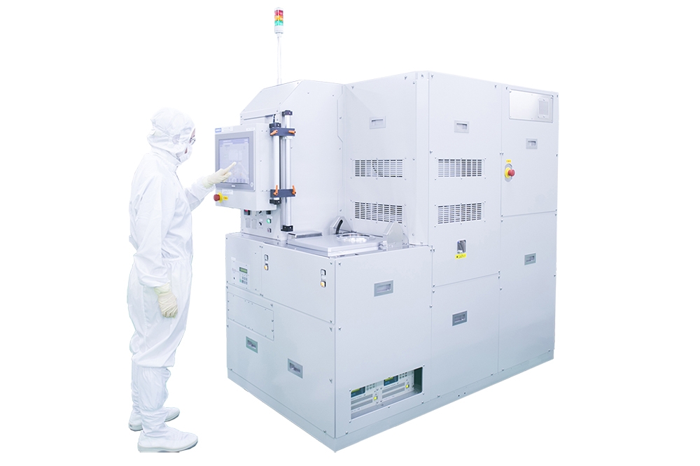
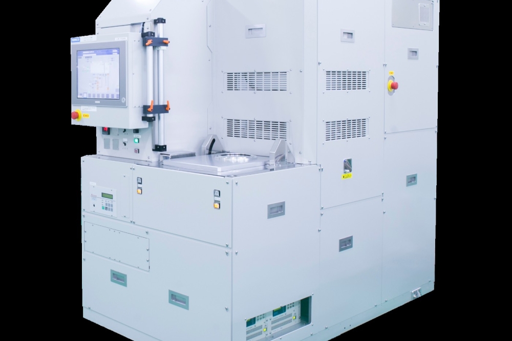
Semiconductor processing equipment company Samco has announced the sale of two of its advanced ICP-RIE systems, RIE-400iP, to III-V Lab, a a research lab based in France. The etching systems supplied will be used in projects aimed at enhancing the performance and integration of III-V semiconductors with silicon.
III-V Lab, a joint lab between Nokia, Thales, and CEA, is dedicated to the industrial research and development of optoelectronic and microelectronic components based on III-V semiconductors. The lab's expertise includes compound semiconductor devices using InP, GaN, GaAs, and GaSb .
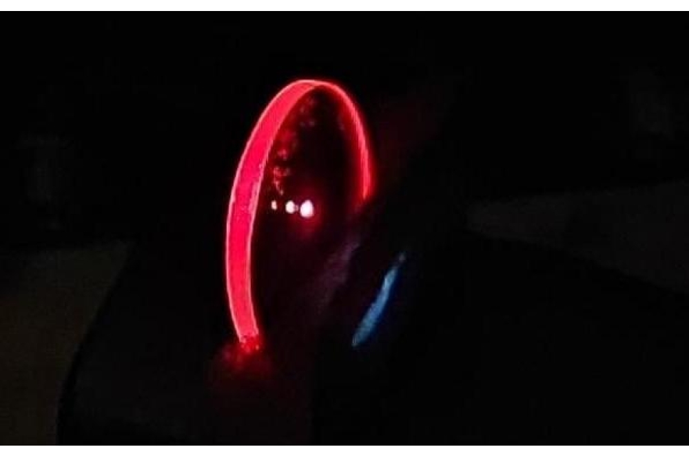
The RIE-400iP is a load lock Inductively Coupled Plasma (ICP) etching system designed to handle wafers up to a diameter of100 mm (4inch). The ICP Source HSTC (Hyper Symmetrical Tornado Coil) is said to effectively deliver uniform, high-density plasma with excellent etch profiles. The system is designed to achieve high productivity for a wide range of etching applications, including InP, GaN, GaAs, SiC, and various materials.
Alexandre Larrue, research engineer of III-V Lab, commented: “Dry etching is a key technological building block for the development of III-V semiconductor innovative devices. The purchase of RIE-400iP ICP etching systems from Samco will allow III-V Lab to address new challenges in compound semiconductor manufacturing and reinforce both its R&D activities and its small volume production. III-V Lab is glad to make the choice of Samco as ICP etching systems supplier.”
Tsukasa Kawabe, president and COO of Samco said: “We are pleased to introduce our top-notch equipment to a new customer in Europe. To date, we have successfully served numerous clients with our expertise in compound semiconductor applications, and we are looking forward to having our systems aid the research into the potential wide-ranging and expanding capabilities of compound semiconductor materials.”