Breakthrough in detecting impurities in GaN crystals
Researchers at Tohoku University develop new contact-less probing technique using light
Carbon impurity has long hindered efficiency in nitride-based electronic and optical devices. But Researchers at Tohoku University, have discovered a method that can quickly detect carbon impurity using light.
Researchers have tried to replicate the high efficiency of blue and white LEDs that use InGaN and GaN, in optical and electronic applications. However, a common issue arises due to carbon impurity, which significantly degrades performance.
Carbon impurity leads to deep-traps, an undesirable electronic defect by which performance is substantially reduced. However, detecting carbon impurity in semiconductor crystals is a time-consuming and costly process. Some methods necessitate creating additional electrodes onto the crystal. Thus, raising costs and inhibiting the inspection speed. Other methods result in the breakage of nitride crystals; therefore, rendering the crystals useless.
Nevertheless, associate professor for the Institute of Multidisciplinary Research for Advanced Materials at Tohoku University, Kazunobu Kojima and his team solved this problem by creating a way to identify carbon impurity using a probing technique using light that makes no physical contact with the crystals. The technique is named omnidirectional photoluminescence (ODPL) spectroscopy.
The process of ODPL firstly involves illuminating a crystal, such as GaN, via external light. The external light is absorbed by the crystal, thereby stimulating it. In order to return to its initial state, therefore, the crystal creates a light to dissipate excess energy.
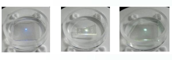
Using the ODPL allows for the quick evaluation of photoluminescence efficiency with high accuracy. Since carbon impurity reduces the photoluminescence efficiency, researchers can also determine the carbon concentration by assessing the PL efficiency. The picture above shows GaN crystals under photo-excitation (carbon concentration level from left to right: high, medium, and low).
Kojima explained the benefits of such a system. "Optical probing technologies are immensely beneficial due to their nondestructive nature. By using light, we can therefore, help detect carbon impurity which is ultimately such a hindrance for GaN devices, such as LEDs and power transistors."


