GaN: Evaluating the reliability of RF devices

Researchers at the International Reliability Physics Symposium highlighted the merits of RF operating life tests of GaN MMICs, the dangers of atomic migration in GaN HEMTs, and how small changes to the thickness of the barrier can have a dramatic effect on device performance
BY RICHARD STEVENSON
GaN is great material for making RF devices. Thanks to attributes that include its ability to operate at a high power density and a high efficiency, it is being deployed in 5G infrastructure, satellite communication and a variety of sensing, targeting and counter-measure applications.
For all these uses, reliability in paramount. In some cases it is critical to providing a satisfactory level of service, while in other circumstances lives depend on it.
Due to this state of affairs, studies of GaN reliability are ongoing, with several recent efforts having just been reported at the IEEE International Reliability Physics Symposium. The intention had been to hold the 58th annual meeting in this series in Texas, in late March and early April. But due to the Covid-19 pandemic, the conference moved on line (delegates could access prepared talks from 28 April until 30 May).
Virtual presentations discussing the reliability of GaN devices in the RF domain included: an account of the virtues of RF operational tests for GaN MMICs; a talk on the dangers of atomic migration of oxygen; and a presentation outlining why increasing the thickness of the AlN barrier can make such a difference to HEMT reliability. Read on to discover the insights from all three papers.
MMICs: DC or RF tests?
For the last sixty years or so, the dominant approach to evaluating the operational lifetime of a MMIC has been a DC accelerated lifetime test of the components. Within every MMIC there are transistors, diodes, capacitors, resistors and metallic interconnects, and each can be evaluated for its failure mechanisms under a DC test. Armed with the knowledge that this brings, it is possible to predict the lifetime of the circuit.
But while this approach is valuable, it has its flaws says Qorvo’s Elias Reese. He posed the question: “What is it that derives the need for something beyond the DC life test?” The answer, according to him, is the RF stresses on GaN circuits.
Although these stresses are not found in many other forms of IC, where signal levels are typically microwatts or milliwatts, they are present in GaN MMICs, where power levels can extend to the kilowatt range. When these MMICs are well-designed, they offer a compact, efficient source of RF power.
To do so, there is an impedance transformation on the chip that enables the RF voltage to great exceed the bias voltage provided. For a high-power amplifier MMIC made from GaN, the bias can be 65 V, while the voltage at the output port can approach 1000 V, creating significant stress.
Stress can also be found in the interconnects. RF signals are not uniformly distributed through the cross-section of a conductive line, but are concentrated at the edges. So, in extreme cases, it is even possible that a line that is not passing any DC current can still fail, due to RF current alone.
Simulating the RF fields in a MMIC is not an easy task. As the components within this circuit have dimensions comparable to the wavelength of the output signal, there are significant variations in electromagnetic field across these building blocks.
“So you have to divide this up into thousands of pieces to accurately calculate the RF voltages and currents across the entire circuit,” says Reese. “That’s a very complex problem, and frankly takes hours and hours of time to solve.”
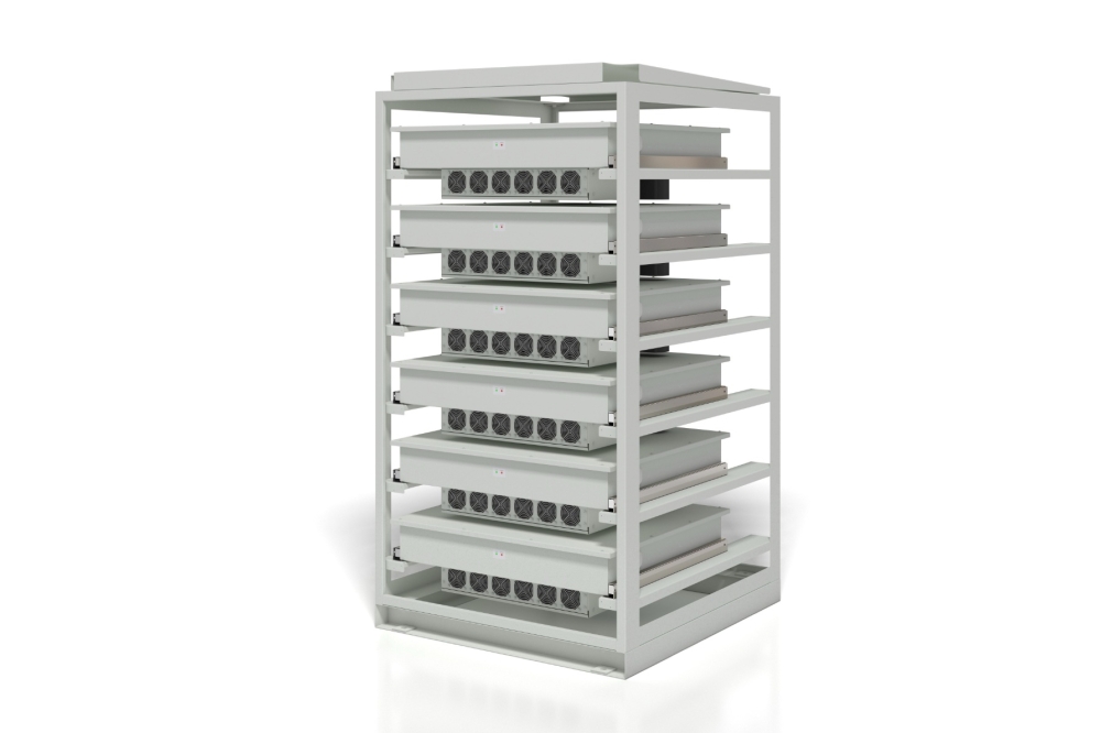
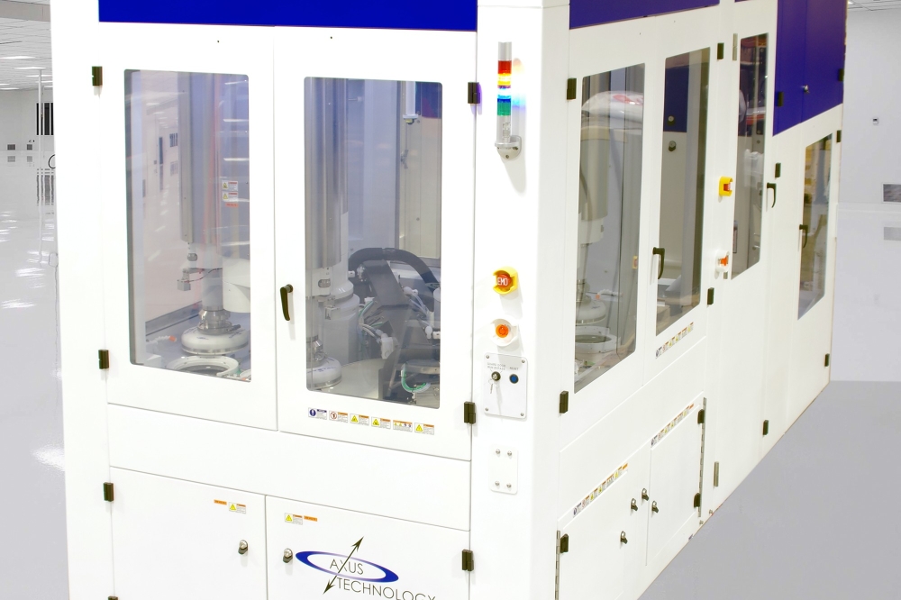
A preferable alternative, says Reese, is the RF operating life test, which is an approach that dates back around 40 years. He detailed an example of this: 24 MMIC high-power amplifiers tested simultaneously for 2000 hours, using prescribed stress conditions and in situ monitoring of key electrical and thermal parameters (see Figure 1).
Although a speedier test is desirable, it is far more complex, warned Reese: “When you try and use accelerating factors such as temperature, you no longer have the ability to hold other factors, such as voltage and current, constant.”
The conclusion to draw is that while RF operating life tests take much time, they provide a level of insight that is not found by other, quicker approaches.
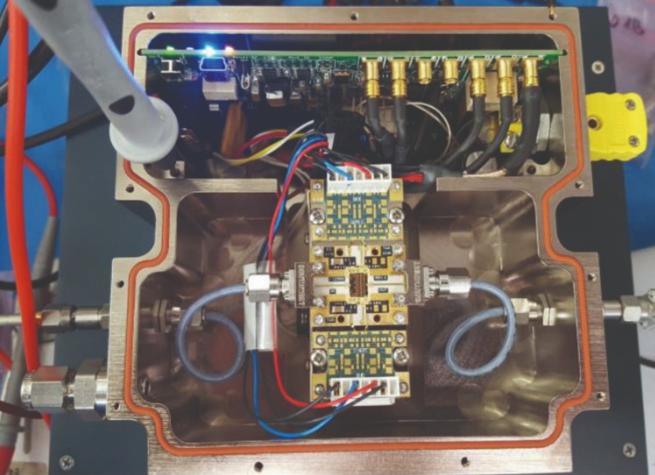
Figure 1. Engineers at Qorvo have conducted simultaneous RF operating lifetime tests on 24 MMIC high-power amplifiers, using independent bias supplies, controls and RF signals.
Scrutinising HEMTs
Efforts at evaluating the reliability of HEMTs with a variety of gate lengths were discussed in a talk given by Enrico Zanoni from the University of Padova. He is working on a variety of European projects, included one that runs from this year until 2023 and is entitled Empowering GaN-on-SiC and GaN-on-Silicon technologies and the next challenging millimetre-wave applications.
In Zanoni’s presentation, he detailed a study of a portfolio of devices made by a collaboration between the team at the University of Padova and colleagues at the IMWS Fraunhofer Institute Halle. The partnership’s investigation included transistors with a gate length of 0.5 µm that could be used for frequencies up to 6 GHz, variants with 0.25 µm gate lengths that can operate at 20-30 GHz, and those with 0.15 µm gate lengths that provide low-noise amplification between 30 GHz and 50 GHz.
Zanoni and co-workers have undertaken extensive testing on their portfolio of devices. Studies have included: 24 hour short-term tests, followed by microscopy, to identify issues related to inter-diffusion; measurements lasting between 500 hours and 4000 hours that consider the impact of elevated temperatures on key electrical characteristics; and an investigation into the impact of carbon-doping levels on short-channel effects in HEMTs with short gate lengths.
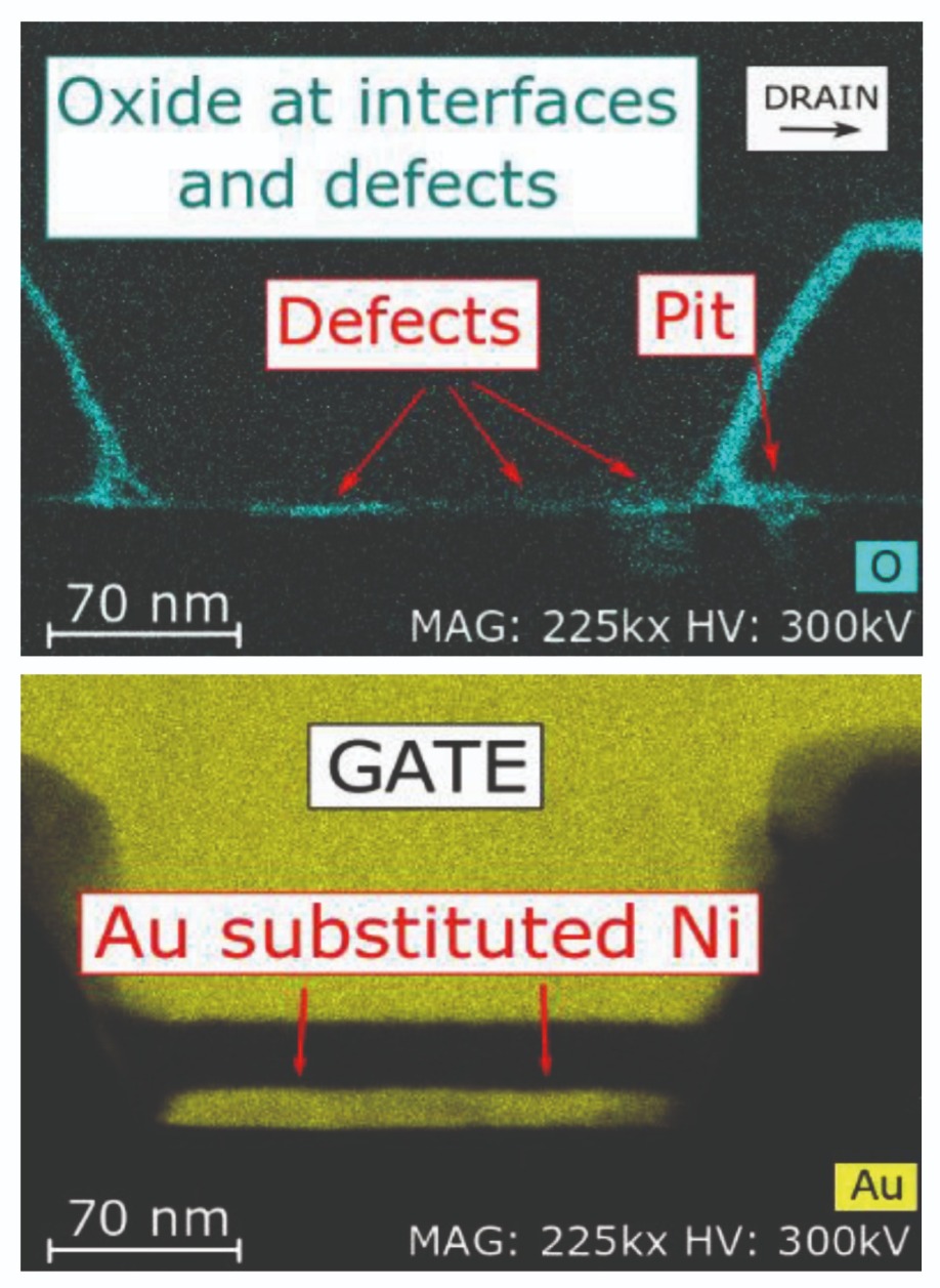
Figure 2. Energy-dispersive X-ray analysis by a team from the University of Padova and IMWS Fraunhofer Institute Halle revealed inter-diffusion issues in first-generation HEMTs. In these transistors, operation at elevated temperatures led to oxygen diffusion under the AlGaN Schottky contact (top) and complete substitution of gold for nickel in the Schottky contact. Gold forms a uniform thick layer.
Fabrication of the team’s first generation of GaN/AlGaN HEMTs with 0.5 µm and 0.25 µm gate lengths included a Ni/Pt/Au Schottky gate metallisation process and passivation by plasma-enhanced, chemical vapour deposition. Engineers found that operating this device at dissipated power levels of more than 25 W/mm in the on-state, a condition that leads to channel temperatures exceeding 250 °C, produced a dramatic reduction in transconductance. Through further investigation, they identified that the impaired performance stems from the combination of a high electric field, a high temperature and a high device current.To identify what is happening within the HEMTs during degradation, the team took the devices, created cross-sections by ion-beam milling, and scrutinised the samples with scanning electron microscopy, transmission electron microscopy and energy-dispersive X-ray analysis. This revealed that gold gradually substituted for nickel in the Schottky contact, and oxygen also caused issues, promoting AlGaN oxidation and pitting.
Second-generation devices have addressed these short-comings by using a different gate metallisation scheme and double-layer passivation. These HEMTs exhibit far smaller changes to transconductance at junction temperatures of up to 250 °C, a result that has led Zanoni to view this as a “pretty robust technology”.
The team have conducted long-term thermal storage tests on this second-generation technology, with HEMTs with 0.5 µm and 0.25 µm gate lengths heated to either 300 °C, 325 °C or 350 °C for 4000 hours. These tests identified a positive threshold shift of 0.2-0.25 V, and a change in Schottky barrier height from 0.84 eV to 0.58 eV followed by recovery to the initial value. The shift in barrier height led to an increase in gate leakage current by one-to-two orders of magnitude; this recovered with a reduction in device temperature.
Further evidence of robustness at elevated temperatures came from DC life tests on these devices, using a range of conditions that included channel temperatures up to 355 °C, drain currents up to 0.3 A/mm and drain source voltages up to 100 V. These conditions produce degradations of below 10 percent in drain current and transconductance.
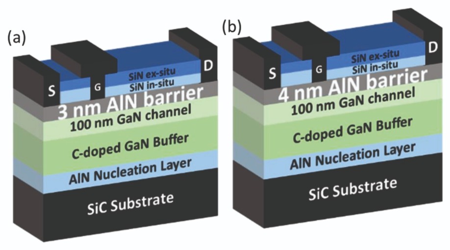
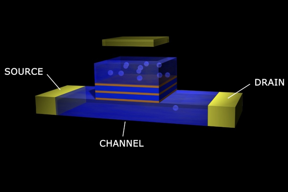
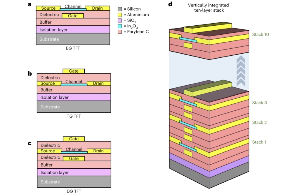
Figure 3. Engineers at Institute of Electronics, Microelectronics and Nanotechnology (IEMN) at Villeneuve d’Ascq, France have compared the performance of HEMTs with 3 nm-thick and 4 nm-thick barriers.
Zanoni and colleagues have also carried out 500 hour RF tests. They employed a junction temperature of 350 °C for HEMTs with a 0.5 µm gate length, and 325 °C for variants with a 0.25 µm gate length. For most devices, RF power fell by less than 0.7 dB, with the magnitude of the reductions in output power correlating with the size of the leakage current. According to the team, when the leakage is higher, more charges are supplied to traps in the AlGaN and buffer layers, leading to an inferior dynamic behaviour. They say that a high electric field between gate and drain is also at play, causing the injected electrons to be highly energetic, damaging the crystal lattice.For HEMTs with a gate length of 0.15 µm or below, short-channel effects can arise that threaten to exacerbate drain-source leakage and shorten device reliability. Strategies for success include adding back-barriers, doping with either carbon or a combination of carbon and iron, and using N-polar AlGaN/GaN channels.
Zanoni and co-workers have considered five different forms of 0.15 mm gate length HEMT. All these devices were made using the same process, the same batch, on epitaxial layers from three different suppliers. For all the samples, peak iron concentration is nominally 2 x 1018 cm-3, while the carbon concentration is either 2 x 1016 cm-3 or 8 x 1016 cm-3.
“Devices with high carbon doping tend to be better,” concluded Zanoni. Current degradation during off-state and on-state stress tests is lower. However, a 24 hour on-wafer test shows that co-doped devices have an inferior performance and reliability to those doped with just iron.
Better barriers
Investigations of the reliability of GaN HEMTs with even shorter gate lengths have been undertaken by a team from the Institute of Electronics, Microelectronics and Nanotechnology (IEMN) at Villeneuve d’Ascq, France. This effort is highly valued, due to the paucity of reliability studies on millimetre-wave GaN devices. The key finding in this study is that the thickness of the barrier, which is highly strained, can govern device reliability.
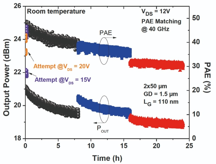
Figure 4. GaN HEMTs with 4 nm-thick barriers show significant degradation in output power and power-added efficiency during a 24 hour stress test.
“The superior robustness when using a thinner barrier is attributed to the reduced strain,” explained team spokesman Raid Kabouche.Fabrication of HEMTs involved processing epiwafers produced by MOCVD and provided by EpiGaN-Soitec.
These epiwafers, grown on 4-inch SiC substrates, consisted of an AlN nucleation layer, a 1 µm-thick carbon-doped GaN buffer, a 100 nm-thick GaN channel, an AlN barrier either 3 nm- or 4 nm-thick, and a 10 nm-thick SiN passivation layer. The latter, added in-situ, provides passivation and reduces surface states.
To create HEMTs from these epiwafers, Kabouche and co-workers etched the SiN layer, before adding Ti/Al/Ni/Au source and drain contacts and an asymmetric self-aligned Ni/Au T-gate (see Figure 3).
Measurements of power performance at 40 GHz were conducted on 2 x 50 µm HEMTs. For the transistors with a 4 nm barrier, an increase in drain-source voltage from 10 V to 20 V led to a fall in power-added efficiency from 50 percent to 45 percent, attributed to device degradation. In comparison, the variant with the 3 nm-thick barrier realised a power-added efficiency of 50 percent at 10 V, and 48 percent at 30 V.
Kabouche and co-workers subjected both types of device to a 24 hour stress test, using a drain-source voltage of 12 V and 8 hour steps, after which the gate voltage is adjusted to maintain a 100 mA/mm drain current. During the course of the test, the power-added efficiency of the HEMT with a 4 nm-thick barrier fell from 45 percent to 30 percent, while the variant with the 3 nm-thick barrier showed no degradation.
In order to further assess the robustness of this structure, the team also performed short-term wafer RF stress tests at baseplate temperatures of up to 140 °C, which correspond to a channel temperature of more than 250 °C. The HEMT with the 3 nm-thick barrier was fully stable at a drain-source voltage of 20 V, but at 30 V significant degradation took place, causing the power-added efficiency to fall from 50 percent to 30 percent. The benefits wrought from reducing the barrier thickness from 4 nm to 3 nm may raise a few eyebrows, given that the critical thickness for an AlN layer grown on GaN is only about 1 nm. However, the team points out that this thickness can be increased to 2-3 nm with a “proper” in-situ cap. This leads to a lower defect density, allowing a HEMT with a 3 nm-thick barrier to withstand a higher electric field and elevated temperatures.
Kabouche revealed that one of the goals for the team is to investigate how the quality of the barrier varies with its thickness. The researchers are also planning to carry out additional on-wafer RF stress tests at 40 GHz, where they do not adjust the gate bias voltage before each step, so that they can observe the impact that this has on the output power density and power-added efficiency. Other intentions are to evaluate larger devices, such as those with dimensions of 4 x 50 µm and 6 x 50 µm, and benchmark other aluminium-rich ultrathin barriers, such as InAlGaN.
Progress by this team from IEMN, as well as that by researchers at Qorvo and the University of Padova, could be reported at next year’s International Reliability Physics Symposium. By then, hopefully the Covid-19 pandemic will be over, allowing experts in device reliability to meet at the Hyatt Regency in Monterey from 21-25 March 2021.


