Allos Semiconductor: Mighty plans for micro-LEDs

GaN-on-silicon wafer developer, Allos Semiconductors, has sold its power electronics and RF business to focus on developing large-diameter epiwafers for micro-LEDs. Compound Semiconductor talks to company co-founder, Alexander Loesing, to find out more.
In July this year, GaN-on-silicon wafer developer, Allos Semiconductors, Germany, revealed it had sold its high power electronics and RF business to Azur Space, a provider of III-V epitaxy for solar cells also based in Germany, for an undisclosed sum.
The move comes at a time when the market for GaN-on-silicon power and RF epiwafers is booming, and merger and acquisitions are rife. For example, just over a year ago, France-based Soitec bought GaN wafer supplier, EpiGaN, for €30m, to strengthen its GaN presence in the RF and power market. Then in Spring this year, ST Microelectronics made its mark on the power market when it acquired a majority stake in GaN innovator, Exagan.
So why sell now? Clearly the timing works for Azur Space. As one of Allos' co-founders, Alexander Loesing, says: “Azur Space has a manufacturing capacity of 500,000, 150 mm wafers a year and wants to leverage its III-V epitaxy skills for the power market.”
“We see a second wave of power electronics businesses that don't want to in-source GaN epitaxy,” he adds. “These companies require a reliable and capable source as they don't want to spend time building up their own epi-supply, so this will be good for Azur Space.”
Alexander Loesing, Allos Semiconductors
Allos also has mighty plans for expanding its micro-LED efforts. Minus its power and RF arm, the company intends to focus its resources on this market, which Loesing describes as 'incredibly intensifying'. “We have three times as much work here than we did only a year ago,” he says,
Over the years, Allos has been building a compelling case for growing micro-LEDs on GaN-on-silicon wafers, instead of the industry stalwart, sapphire. But how exactly does the company intend to make its mark on the fast-growing, highly competitive world of micro-LEDs?
Making the difference
To reach mass sapphire-based micro-LED production, industry players are busy addressing manufacturability issues, including yield and cost. For example, GaN-on-sapphire LED chips are processed on 100 mm and 150 mm diameters. Larger wafers are too expensive to be used in LED manufacturing, and also suffering from bow, leading to lower yields.
Meanwhile, inhomogeneities in the emission wavelength of a typical GaN-on-sapphire LED epiwafer mean chips need to be tested and sorted into bins to ensure the micro-LEDs emit the desired colour. Given a 4K display comprises some 25 million micro-LEDs, this process of binning clearly isn't viable at volume production.
“The industry needs to move towards an epi-growth and chip processing environment that delivers large diameters with a high uniformity to avoid the need for binning, and at high yields,” highlights Loesing. And the Allos director is sure that his company's hetero-epitaxial GaN-on-silicon growth process will make the difference.
According to Loesing, the epi-growth process uses strain engineering and lateral overgrowth to overcome the lattice mismatch and thermal expansion differences between GaN and silicon that would otherwise lead to wafer bow, cracks, poor crystal quality, and associated wavelength non-uniformities and yield loss.
As part of the company's method to achieve high crystal quality, epitaxial lateral overgrowth is used, which is analogous to the patterned sapphire substrates used in sapphire-based LED manufacture to reduce GaN crystal defects. Careful strain balancing introduced during epi-growth helps to control bow and deliver flat epiwafers after growth. And the company also uses its proprietary and patented strain engineering to precisely control heat across the entire wafer diameter during temperature-sensitive InGaN multi-quantum well growth, promoting wavelength uniformity and reproducibility from wafer to wafer.
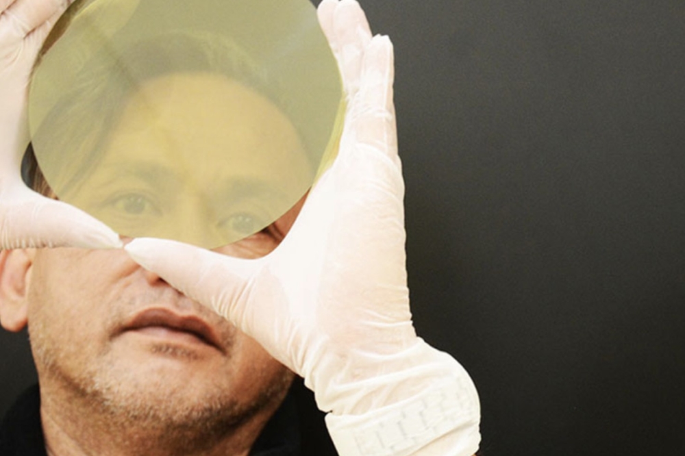
A 300 mm GaN-on-silicon epiwafer for micro-LEDs from Allos Semiconductors.
“This strain engineering and crystal quality challenges are much more difficult in LEDs compared to power electronics, but this is good for us,” says Loesing. “Very few companies can use GaN-on-silicon to make LEDs with our levels of quality, and I haven't seen anyone come close to the uniformities that we are showing.”
Indeed, at 2x108 cm–2, the crystal quality of its GaN-on-silicon substrates is on par with that of market-leading GaN-on-sapphire. Epiwafers are coming through crack-free with minimal bow while wavelength uniformity is stable with nearly 98% of wafer areas hitting targets.
As Loesing also points out, silicon substrate removal via grinding and etching, as used in silicon lines, is more straightforward than the laser lift-off necessary to remove sapphire substrates from chips. And epi-growth takes place in standard MOCVD reactors on 200 mm and 300 mm wafers, opening the door to micro-LED production on low-cost, high yield, silicon processing lines.
Still, without a doubt the micro-LED world is very much entrenched in sapphire. To tackle tradition, Allos is working to ensure a steady supply of GaN-on-silicon epiwafers. “We need to make sure we can provide enough samples to our customers,” says Loesing.
Given time, the company director is confident that micro-LED players will make the move from sapphire to GaN-on-silicon. “If we'd spoken four years ago I would have said I don't believe that the LED industry will ever take-up GaN-on-silicon as companies were focused on throughput,” he says. “But the arrival of micro-LED displays has changed this, and high yields are the crucial to drive costs down - our technology ensures this with wafers, and all subsequent processing steps.”
So what now for Allos Semiconductor? Right now, the company is working on, as Loesing says, 'results'.
Indeed, since the sale of its power electronics and RF arm, Allos has announced that it is working with researchers from King Abdullah University of Science and Technology (KAUST), Saudi Arabia, on high efficiency nitride-based red LEDs on silicon. Professor Kazuhiro Ohkawa from KAUST has already grown InGaN-based red LEDs on sapphire and working with Allos, intends to do the same on silicon.
“We continue to push forward and look forward to showing more results, and also to making new announcements about customer collaborations very soon,” says Loesing. “This micro-LED market is exploding and I'm having the most fun at Allos that I've ever had.”


