Oxford Instruments and LayTec collaborate on front end processing

Companies to work together to provide plasma process solutions with in-situ metrology for production of compound semiconductor devices
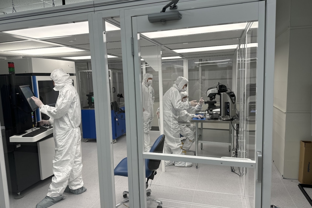
Two technology leaders within the compound semiconductor industry, Oxford Instruments Plasma Technology and LayTec announce an exclusive collaboration agreement to enable the next generation requirements of advanced semiconductor devices in the high-volume manufacturing (HVM) environment. The partnership aims to develop and integrate LayTec’s accuracy and control with Oxford Instruments’ wafer processing expertise.
Together, they will combine plasma process solutions with proven in-situ metrology to achieve next generation device performance and enable a repeatable HVM process to shorten customers’ yield ramp. LayTec will develop the in-situ metrology while Oxford Instruments will integrate LayTec’s control with its advanced wafer processing solutions to deliver an enhanced solution to the customer.
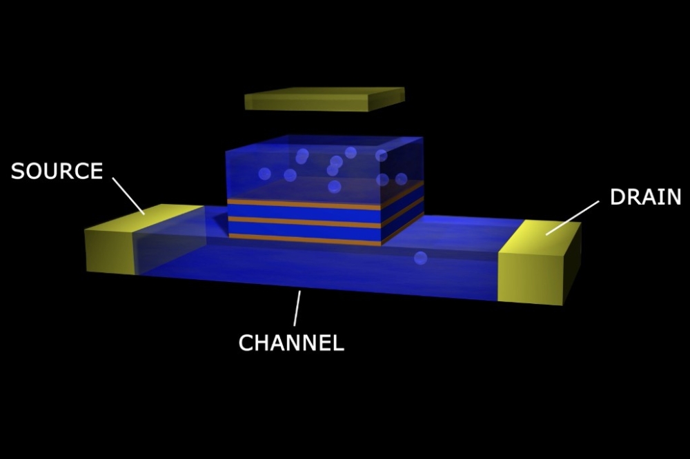
Driven by market demands for efficient power conversion, the IoT and datacomms compound semiconductor devices based on materials such as GaAs/InP, SiC or GaN, are becoming increasingly used due to their superior performance. However, challenges remain to move the technology from small prototypes to wafer scale, HVM. While device dimensions are relatively large, the often-complex layer structure means that acute accuracy of processing within these layers is required to realise the required process stability and yield to drive down the cost per wafer and accelerate adoption into the target application.
Volker Blank, CEO, LayTec comments: “LayTec is very excited to take the next step in widening its product portfolio with an innovation leader like Oxford Instruments. This technology partnership allows us to expand further along the process chain in one of our traditional core markets by applying our key knowledge of data analysis and integration of customised high-precision optical metrology systems. After serving our customers in the compound semiconductor industry for more than two decades, we look forward to this new opportunity to support our customers in further processes and device optimisation.”
Frazer Anderson, innovations & solutions director at Oxford Instruments states: “This is a crucial next step in the implementation of our product development strategy and the accelerated timing reflects the recent momentum we’ve seen in the markets we serve. It also underlines our commitment to deliver continuous productivity improvements to our customers.”
Anderson continues: “As we enter a very exciting period of innovation and growth, it is our firm intention to meet the requirement of improved performance and reduced cost of ownership objectives necessary to support needs of the emerging GaN power and RF market. This collaboration with LayTec will further increase our ability to be able to deliver both requirements.”
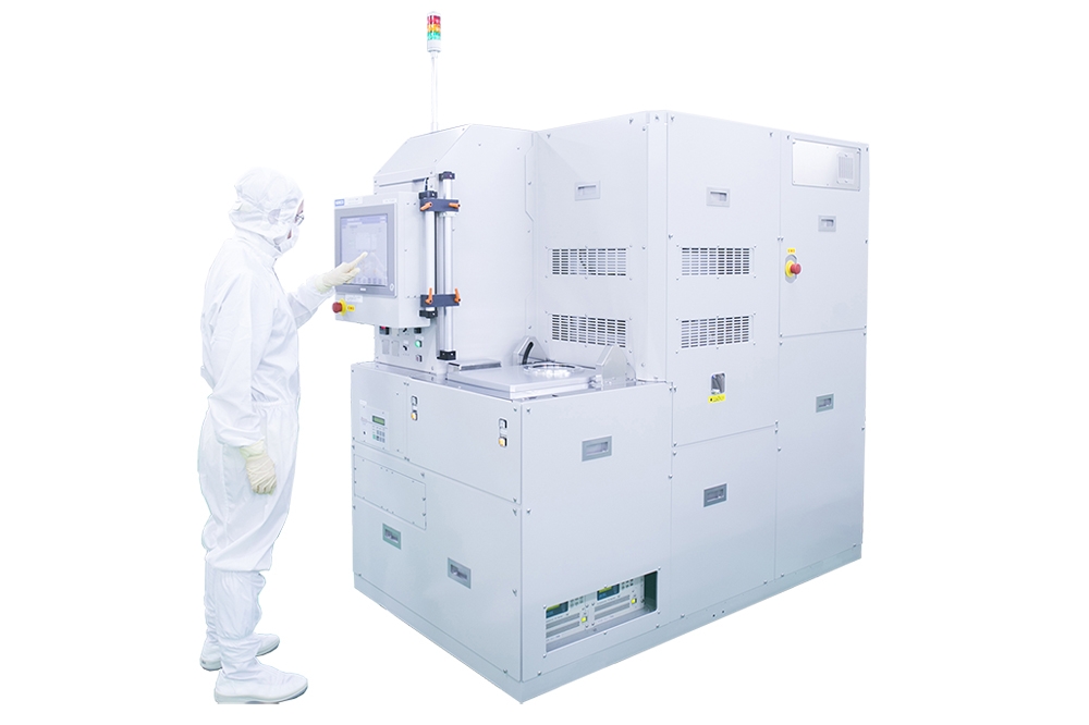
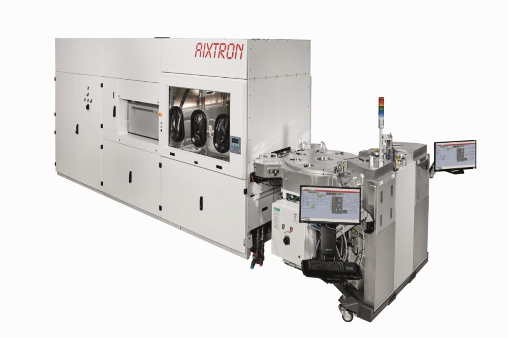
Oxford Instruments is a recognised technology leader in compound semiconductor processing with a range of proven wafer processing solutions installed at HVM customers. Combining Oxford Instruments’ stable plasma processing platform with LayTec’s innovative and precise end point technology in plasma etching applications allows the control and repeatability needed to increase the wafer-to-wafer yield.
The synergy of joint development and exclusive supply agreement will allow the expertise in both companies to develop and supply unique HVM ready solutions for the evolving needs of the compounds industry. The long-term agreement will cover developments on the entire range of Oxford Instruments’ plasma etch and deposition systems with shared rights to the Intellectual property (IP) produced and co-ordinated marketing activities. The delivery of the first joint customer solution is targeted for H2 of 2021.


