Enhancing volume production of microLEDs and lasers
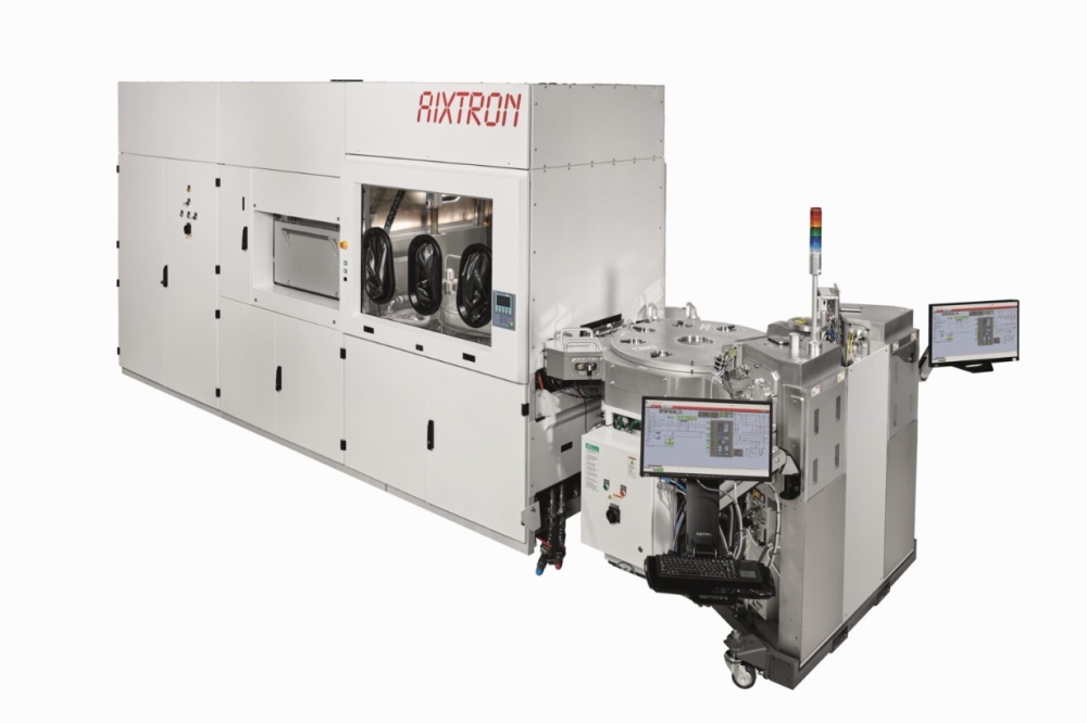
Aixtron’s new fully automated G10-AsP platform, the largest 200 mm AsP batch reactor released to the market, will initiate the end of the wafer binning era.
By Vincent Meric, THOMAS KORST and Arthur Beckers from AIXTRON SE
Compound Semiconductor devices have come a long way from the first transistors and lasers used in the 1990s for telecommunication or from the replacement of incandescent light bulbs at the beginning of the millennium. They are now extending the roadmap of many applications from power electronics to advanced photonics devices, opening up one opportunity after another: while VCSELs and edge-emitting lasers have a bright future in lidar for autonomous vehicles, microLEDs have the potential to disrupt the market for displays.
Fast growing demand from multiple applications drives chipmakers to employ high-volume, mass production processes. These processes must be tailored to the specific requirements of each device type and be robust enough to ensure high yields in a manufacturing chain with growing complexity. To address all these needs, Aixtron has launched a new MOCVD platform for arsenide-phosphide epiwafers for microLEDs and lasers.
This new MOCVD platform AIX G10-AsP brings full automation, automated cassette-to-cassette wafer loading and in-situ etching for the first time to the epitaxy of arsenide-phosphides. These features will help to ensure reliable, efficient production of high-quality microLEDs, VCSELs and InP lasers with enhanced uniformity, reduced particles and optimised yield.
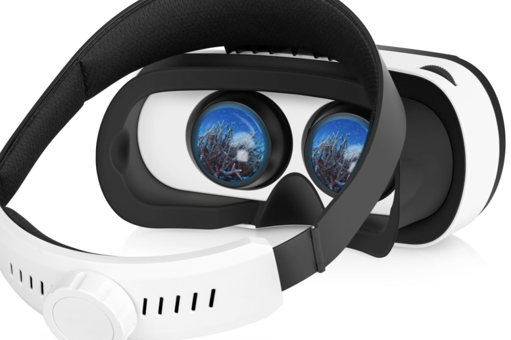
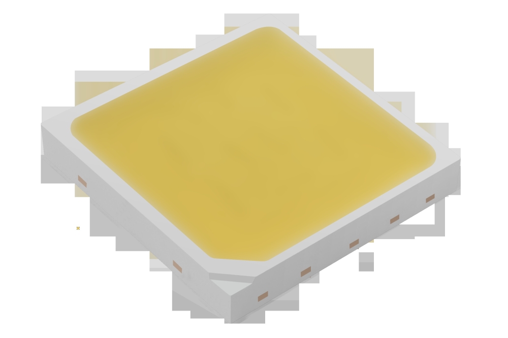
MicroLEDs are on the verge of revolutionising the display industry
Since the emergence of the solid-state lighting era a decade ago, LEDs have found their way into several other applications, including the head and tail lights of automobiles and the backlighting units for displays. In addition, LEDs have been deployed in industrial displays and signage, with red, green and blue pixels mounted onto a thin-film transistor backplane to deliver very bright, high-resolution displays. These displays are used for advertising, both indoors and outdoors.
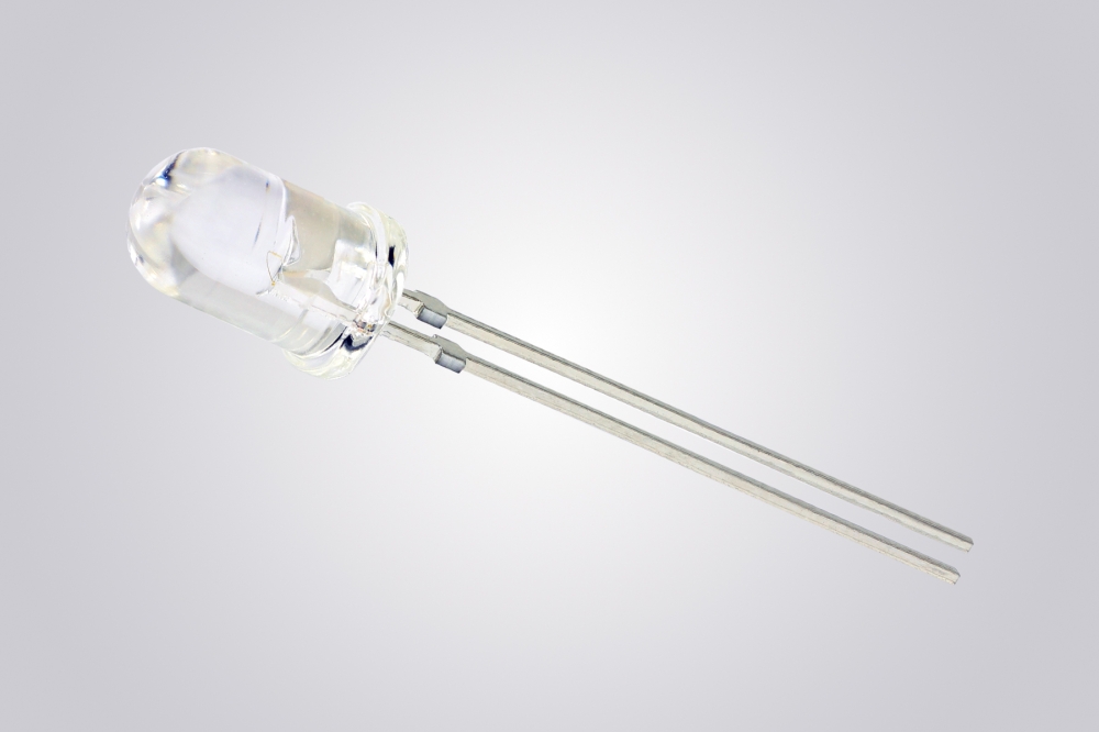
Recently, one of the most exciting activities within the LED community has been the development of the microLED, a miniaturised form of this device. It is no more than 50 µm in width, and in some devices this dimension can be as small as 600 nm, according to a recent report from Yole Intelligence.
MicroLEDs are seen as the future of displays. Compared with organic LEDs, these inorganic siblings are renowned for their durability, their long lifetime, and their absence of burn-in effects. What’s more, microLEDs promise to be far more energy efficient, brighter, and able to offer a wider high dynamic rate and a more extensive colour gamut, thanks mostly to their intrinsic, superior quality over organic material. In addition, due to diminutive dimensions, microLEDs are expected to enable low fill factors – less than 10 percent for larger displays – opening the door to integrate new sensors between the pixels.

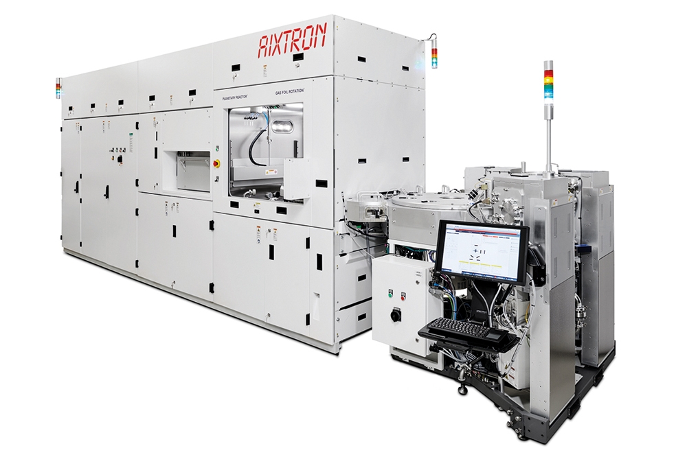
G10-AsP fully automated processes with cassette-to-cassette handling and optional standard mechanical interface port
Due to their tremendous promise, the last few years have witnessed a great deal of research and development of the microLED. This miniature marvel is seen as a very promising light source for smart watches, smartphones, TV displays, augmented-reality projection displays and automotive displays. With so many lucrative opportunities on the horizon, the microLED has the potential to become the biggest market opportunity for the LED over the next decade.
Fulfilling the commercial promise of the microLED hinges on overcoming several challenges, both related to quality of the pixels and their transfer to backplanes. To enable a very high pixel resolution and a low manufacturing cost, chipmakers will have to produce very small pixels and transfer them to the final display. It is anticipated that pixel sizes of not much more than 10 µm are needed for first-generation volume products addressing mid-size and larger displays, and variants with a width of less than 3 µm – and possibly sub-micron – may be required for very high-resolution AR applications. Manufacturing pixels that are this small is challenging. It is crucial to break new ground for the defect density at the epitaxy level, not only to ensure a high chip yield, but because this matters for the final display.One downside of the miniaturisation of the LED is that it impairs binning, with small pixel sizes preventing any sorting of this device. It may be possible to introduce techniques that repair pixels or deal with redundancy – both are under development – however, this is undesirable in the long run because any such solution will increase production costs.
Another substantial challenge for making displays from microLEDs is that it requires the transfer of a vast number of devices. For example, to produce a 4K TV, there needs to be a transfer of around 25 million sub-pixels, which is too many for traditional pick and place. Superior techniques may come from new transfer methods, such as elastomer stamps and even microfluidic or laser transfer. Another option, suitable when a very high density of pixels is needed for a small display area, is the direct bonding of microLEDs to a CMOS wafer. Ultimately, all the approaches advocate for a leapfrogging improvement in wafer-level uniformities and cleanliness.
Advanced photonics requirements
In contrast to microLEDs, photonic devices are well established, having served in several applications for many years. For example, infrared compound semiconductor lasers and detectors are the building blocks of telecom and datacom transceivers supporting the world’s hunger for data, year after year. For telecommunication, an increase in data rates will come from a hike in bandwidth, realised by increasing the number of different wavelengths transmitted simultaneously through an optical fibre.
To ensure denser packing of distinct frequencies, engineers have been trying to increase the tightness of the wavelength tolerances, to prevent overlap between a signal at one wavelength and a signal at another. Fabrication of these photonic devices is a highly complex process, often requiring several growths in an MOCVD reactor.
This complex manufacturing calls for refined control of the epitaxial process, in terms of material accuracy and defects. If any yield loss occurs during one of the earlier steps, it is particularly detrimental, having a multiplier effect on any subsequent step.
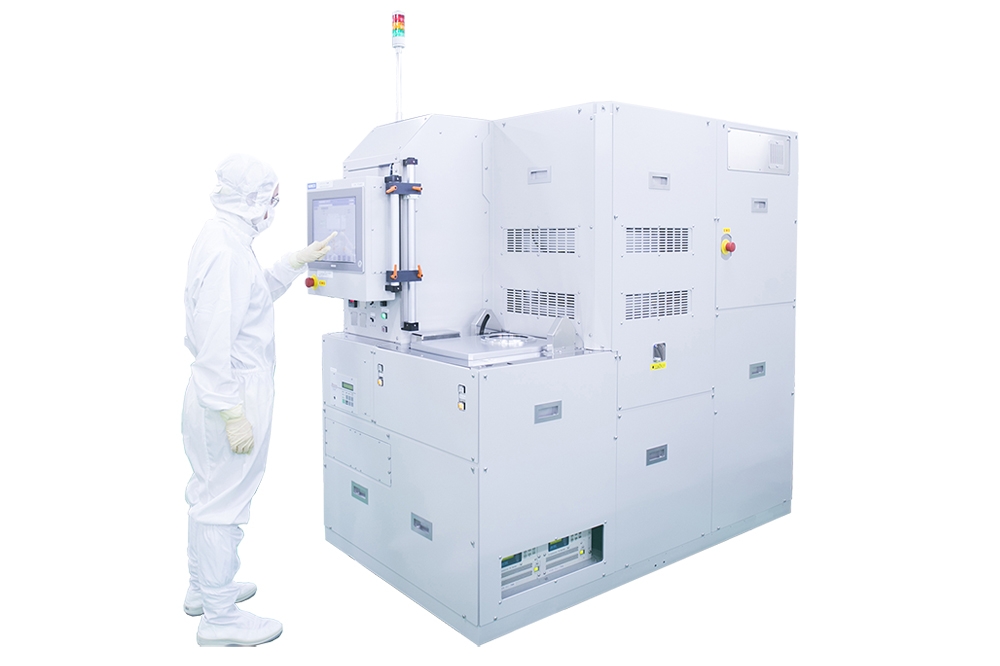
The new G10-AsP: World’s first fully automated AsP MOCVD reactor
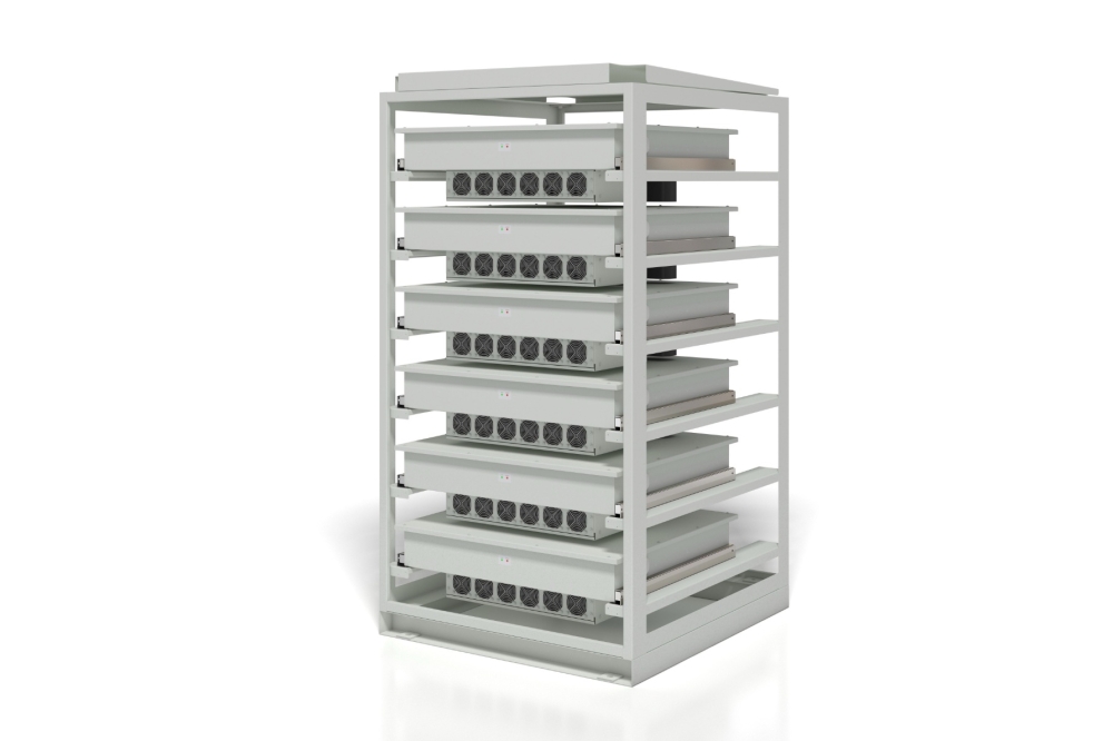
Aixtron is releasing the first fully automated AsP platform, the G10-AsP. Engineered to serve the most demanding microLED and advanced photonics requirements, this system features a cluster of two process modules, each embedding a mini-batch reactor that accommodates up to twelve 4-inch, eight 6-inch or five 8-inch wafers. The platform inherits some of the AIXG5+ C DNA and architecture, such as its level of automation and in-situ cleaning.
Equipped with automated, high-temperature, cassette-to-cassette loading of wafer, the G10-AsP can undertake up to ten process runs – that is, for example, the production of fifty 200 mm epiwafers – before there’s any need for operator assistance to load new wafers. This exceptional degree of automation enables a reduction in the number of technicians required to provide support around the clock, day after day.
For the first time, the front-end of the MOCVD system can be equipped with standard mechanical interface pods to minimise the exposure of epitaxial wafers to the room environment. Aided by this and in-situ cleaning, particle densities can plummet as low as never before for MOCVD processes. For example, the G10-AsP has demonstrated an average defectivity below 0.1 defects/cm² with a particles size greater than 2 µm in a 80-wafers marathon campaign (see Figure 1).

Figure 1. G10-AsP demonstrated defectivity level, on-wafer and in 10-run marathon mode (R-E-R).
With on-board in-situ cleaning, users can reset chamber conditions on demand. They may decide to do this after every process run, if they need to cater for the most demanding requirements; or they may do so after completing a production campaign, so they benefit from the highest throughput.
Note that the benefits of in-situ cleaning minimise imperfections in the epiwafers. Another benefit of the cleaning process is that it can replace the regular preventive maintenance for any AsP MOCVD system – this is required to remove contaminated material from the chamber on a regular basis. Eliminating preventive maintenance on the process chamber ensures a significantly longer, more stable production campaign for all types of MOCVD process.
The G10-AsP also inherits the advanced wafer-level temperature control that has been a reliable component of Aixtron reactors for growing nitride wafers. This enables individual control of wafer temperature, ensuring improved reproducibility in campaign mode. Another feature of the G10-AsP is a new central gas injector that provides the highest metalorganic and hydride utilization. With this refinement, chemical efficacy is improved by more than 40 percent. Therefore, purification and scrubbing costs are trimmed to the lowest ever seen for such materials.
What’s more, the tuning capability of the new injector enables new levels of uniformity for multi-quantum wells, and for quaternary materials used for advanced lasers. For example, trials have demonstrated exceptional uniformity of the platform, with close to 100 percent of the surface area within a 3 nm-wide bin (see Figure 2) over a campaign of twenty-one 200 mm wafers (fully and partially load combined).

Figure 2. Wavelength uniformity yield for microLED wafers (5 x 200 mm).
Equally impressive results have come from 150 mm VCSEL epiwafers. In this case the uniformity is as low as 0.7 nm standard deviation within wafer, translating into yields as high as 100 percent for a 6 nm-wide bin in a 80 wafers marathon campaign (see Figure 3).
For both microLEDs and today’s advanced photonics, the era of wafer binning is now over. The high volume of compound semiconductor devices needed for markets demands scalable, reliable MOCVD processes. Offering just this is the G10-AsP: it can provide the production of microLEDs with sizes of 10 mm or less; and accommodate the complex requirements for high-volume production of InP edge-emitters and GaAs-based VCSELs, with the controllability of regrowth only MBE could reach today.

Figure 3. Wavelength uniformity yield for processed VCSEL wafers (8 x 150 mm).
The G10-ASP is the largest 200 mm AsP batch reactor released to market, enabling the highest throughput of its class to maximise cleanroom utilisation. As chipmakers undertake a rapid adoption of the G10-AsP system, they will fulfil the tightened market requirements for microLEDs and lasers and enable the production of high performance, predictable devices while realising significant cost savings.