Delving into the details of the GaN power electronics patents war

While accusations fly of disloyal employees and a lack of manufacturing knowhow, what will really matter in an IP war is the fine print in the patents.
BY RICHARD STEVENSON, EDITOR, CS MAGAZINE
The commercialisation of different classes of GaN devices seem to follow a similar trajectory. For the first major technology, the GaN-based high-brightness LED, the opportunity for lucrative sales spurred many companies from all over the world to launch products to market. Initially the efforts of these companies focused on improving product portfolios and revenue, but once sales had climbed, they started to wage war with one another, claiming infringement of key patents. Now it looks like history is starting to repeat itself, triggered by surging sales of GaN power devices.
The first significant shots in this sector were fired late this May, when the Californian fabless firm EPC issued a press release stating it sued Chinese chipmaker Innoscience for infringing four of its US patents. EPC claims that Innoscience is drawing on this IP for the production of its 100 V and 650 V products.
As well as filing complaints in the federal court and with the US International Trade Commission, EPC publicly accused Innoscience of poaching two employees that went on to be that chipmaker’s CTO and Head of Sales and Marketing – hires that are said to be behind the launch of very similar products.
Innoscience did not take long to respond to EPC’s accusations. The vertically integrated device manufacturer issued its own press release just two days later, saying that it had conducted a thorough analysis and found no infringement.
While throwing accusations around may help to strengthen a company’s credibility, what will actually matter in this war is the fine print within the patents. They are not discussed in detail in the press releases from EPC and Innoscience, but have been examined by patent litigators Radulescu LLP; and in a recent webinar this firm’s leader, David Radulescu, shared his thoughts. Radulescu is well-positioned to comment on such matters – he is neutral in this battle with a great deal of relevant expertise, having spent many years advising and representing GaN LED companies fighting disputes over claims of infringement of intellectual property.
David Radulescu has a PhD in compound semiconductors and devices (HEMTs) from Cornell University so he is uniquely positioned to separate the wheat from the chaff from both a legal and technical perspective simultaneously.
The case between EPC and Innoscience considers just one of many classes of GaN transistor. Both parties produce devices that are normally off (E-mode), and feature a p-doped layer of (Al)GaN under the gate of the device.
EPC holds a total of 57 US patents, and its action against Innoscience involves four of them – two from 2013, and another two from 2017.
One of the patents from 2013, the US 8,350,294, concerns the design and fabrication of a compensated gate MISFET. A key issue here, according to Radulescu, is whether the phrase ‘compensated GaN layer’ describes the gate layer in Innoscience’s devices, which are presumably formed by doping GaN with magnesium. Realising effective p-type doping is far from trivial. It was a key milestone in the development of the LED, with one of its pioneers, the Nobel Prize winner Shuji Nakamura, discovering that annealing in a nitrogen environment breaks up magnesium complexes, drives hydrogen out of the material and ultimately improves its conductivity.
Radulescu shared snippets of articles in the public domain that have been written by employees at Innoscience and discuss the use of a magnesium-doped p-type layer beneath the gate. In addition, he highlighted results of secondary ion mass spectrometry (SIMS) carried out by EPC, looking at levels of magnesium, oxygen, carbon, aluminium and hydrogen in the gate stack of an Innoscience device.
The expert in patent litigation explained that the court will have to mull over a number of questions. As well as considering whether Innoscience’s devices use a ‘compensated GaN layer’, they will have to try and determine how the company makes its p-type GaN stack – is there a post-growth anneal in nitrogen, mirroring LED production – and what can be concluded from the SIMS data.
EPC’s other patent from 2013 that is claimed to be infringed by the actions of Innoscience is that associated with a self-aligned gate E-mode HEMT (US 8,404,508). In this patent, EPC states that its self-aligned process leads to the bottom of the gate (contact) metal having the same dimension as the top of the ‘gate compound’.
Radulescu pointed out that gates can have a variety of shapes, including a self-aligned geometry and a regular and inverted T-shape. Innoscience has a patent for its gate process (US 10,971,579). With this approach, the GaN beneath the gate is intentionally made wider than the gate (contact) metal.
According to Radulescu, a key question facing those that are trying to evaluate the validity of EPC’s claim of infringement of the patent ‘508 patent is this: Does ‘etching away the doped GaN layer, except a portion of the doped GaN layer beneath the gate contact,’ describe Innoscience’s process that results in a gate ‘ledge’?
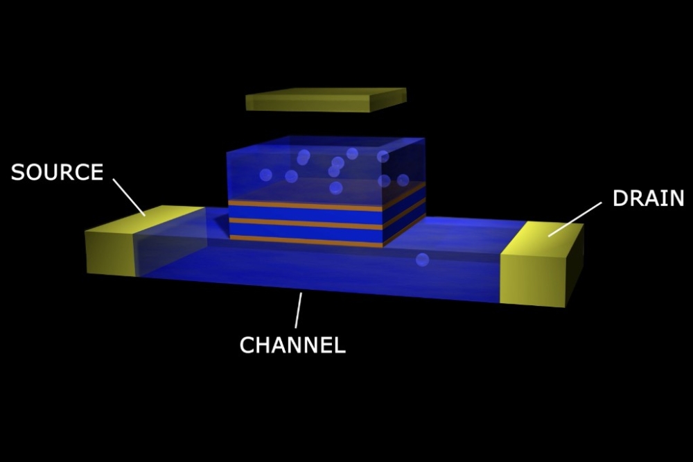
The remaining two of four asserted patents are from 2017 – US patents 9,748,347 and 10,312,335 – and cover a gate with self-aligned ledges for enhancement-mode GaN transistors. These patents describe an architecture for trimming the gate leakage current: a ledge beneath the metal gate that features side surfaces ‘extending horizontally’ towards the source and drain (see figure).
EPC has two patents that detail how to cut the leakage current of E-mode GaN HEMTs with an architecture that uses gate ledges and side surfaces that extend horizontally.
Radulescu remarked that both patents require gate ‘side surfaces’ that ‘extend horizontally’ towards the source/drain. It is possible Innoscience will argue that its side surfaces are close to vertical, or it may question how one should define the required slope.
What is clear is that the legal process will take a great deal of time and money. A healthy budget for litigation is critical, the chances of success are far higher with a legal team experienced with GaN technology and devices, and it’s crucial to avoid strategic mistakes during the process.
The hearing of evidence in this case is scheduled for next February, with a target date for a decision of 3 October, 2024. Should EPC win, Innoscience will be prevented from exporting products to the US.
Drawing on the history of the LED, one should expect that this patent battle will be the first of many associated with the GaN HEMT. And while there will be some winners and losers, many outcomes may not so clear cut, with cross-licensing deals set up that have pros and cons for both parties.


