Amberwave details compounds-on-silicon strategy
by Michael Hatcher
The US National Science Foundation (NSF) has handed collaborators at Amberwave Systems and the Rochester Institute of Technology (RIT) $300,000 for a three-year project designed to improve silicon device performance through the integration of III-V materials.
Amberwave, whose past achievements include pioneering the development of strained silicon, has already invented a new concept that can "trap" defects created by the lattice mismatch between silicon and other semiconductor materials like GaAs and germanium.
The NSF grant will be used to further develop that technology, and apply it to high-quality device structures for the first time.
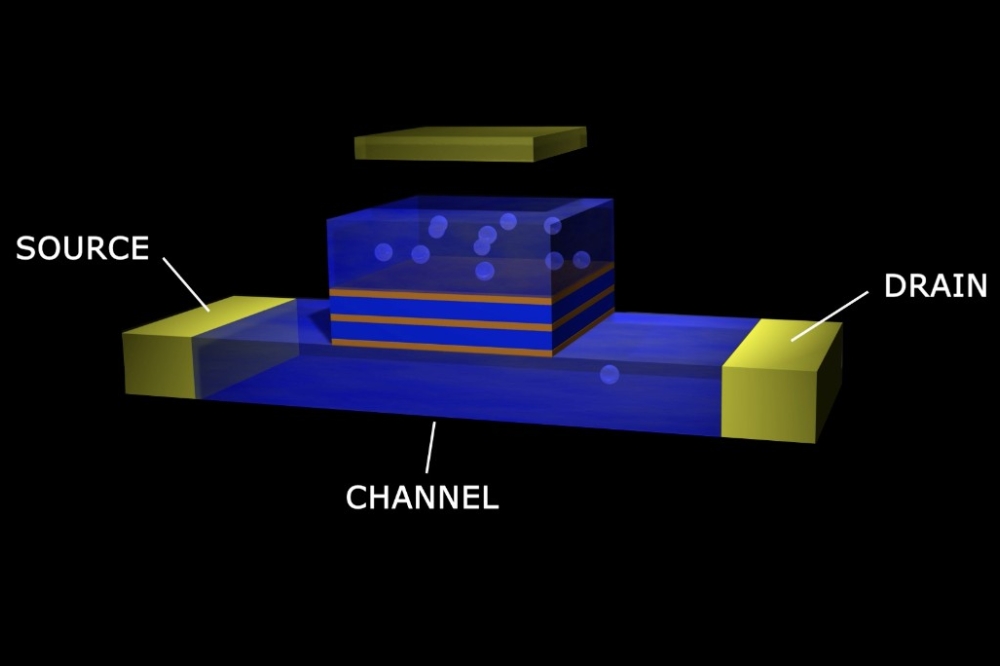
Known as "aspect ratio trapping" (ART), the defect-limiting technique could be used to improve field-effect transistors and resonant tunneling diodes, devices that could play a key role in high-performance memories.
Just like the recently announced DARPA program known as "COSMOS" (see related story), the key aim behind the project is to integrate high-performance material benefits with conventional CMOS-style processing.
Tony Lochtefeld from Amberwave believes that the NSF project highlights the natural evolution of the semiconductor industry:
"Improving CMOS performance through the addition of new materials is becoming more and more important," he said. "Adding III-Vs to silicon to exploit their unique functionality is a natural extension of this trend."
Caught in a trap
So far, Amberwave s research team has been able to trap crystal defects arising from the lattice mismatch of germanium and III-Vs grown on silicon to within the first "few hundred nanometers" of the epitaxial growth.
Because the defects are also confined laterally, to the sidewalls of narrow openings in a dielectric mask on a silicon wafer, it is possible to fabricate device structures on the defect-free "stripes" that remain.
The stripes so have to be fairly narrow - Lochtefeld says no wider than 0.5 µm - but this is enough room on which to fit devices like field-effect transistors or resonant tunneling diodes (RTDs).
Other attempts to reduce the effect of the lattice mismatch have tended to focus on depositing much thicker films of the compound material, says Lochtefeld, adding that this approach tends to lead to film cracking.
RTDs are the initial target for commercial applications of the defect-trapping approach, and could be seen in around five years from now.
"RTDs have great potential, when combined with silicon CMOS, to reduce transistor count and improve performance for key logic functions," explained Lochtefeld.
Perhaps most importantly, he says, the area and power consumption of static random access memory (SRAM) cells could be cut by more than half.
While this idea has been around for a while, it has so far proved impossible to make high-quality RTDs on anything except a III-V materials platform.
Smaller memories
Lochtefeld says that cutting SRAM cell area would be an especially useful application of ART s defect-trapping abilities. "First, SRAMs are critical for fast embedded microprocessor memory, and SRAM arrays are occupying progressively larger portions of modern microprocessors - now on the order of half of the die area."
"Second, RTDs can have a very small footprint - defect-free regions of III-V material such as those already demonstrated on silicon using ART are more than large enough."
Of course, there are still significant technological challenges to overcome. The immediate challenge, according to Amberwave, will be to planarize the islands of III-V material for subsequent device fabrication.
And, because RTDs are so sensitive to tiny variations in the epi structure, achieving a good enough deposition uniformity across a 300 mm diameter wafer will probably be the toughest challenge of all.
Author
Michael Hatcher is the editor of Compound Semiconductor magazine.


