Dual integration aims for 100Gb/s economy
A European project has gained €3 million ($4.7 million) in EU funding to help show that increased optical integration can drive down the costs of 100 Gbits/s networks.
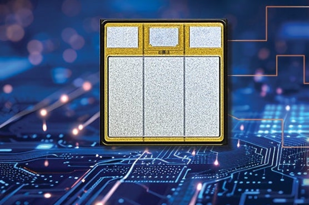
From its start on April 1, the three-year APACHE project has tackled this challenge from two directions, monolithically integrating extra functionality into InP chips and then combining these onto silica waveguides.
“The theme of APACHE is to develop components to deal with advanced modulation formats for much higher speed networks," explained Graeme Maxwell, the project's technical manager. "We're also looking to develop components that run with low power consumption."
“The philosophy is to develop the highest level of functionality that we can in a cost-effective manner by marrying together the best from monolithic integration with the best from hybrid integration."
The physical integration will be performed by the Heinrich Hertz Institute (HHI) in Berlin, Germany, and the Centre for Integrated Photonics (CIP) in Ipswich, UK, where Maxwell is based.
For one project goal, APACHE aims to monolithically integrate arrays of InP lasers for wavelength division multiplexing (WDM), while in another it will similarly integrate arrays of WDM receivers.
Another key InP integration goal involves the fabrication of “nested" Mach-Zehnder modulators to allow multi-level modulation schemes such as quadrature phase-shift keying (QPSK). Other modulators for differential phase-shift keying (DPSK) and on-off keying (OOK) will be made in InP rather than conventional lithium niobate.
Refinement of CIP s silica-on-silicon waveguides "“ Maxwell describes them as the optical equivalent of a printed circuit board "“ for 100 Gbit/s networks will allow straightforward optical interconnection of the semiconductor devices in APACHE's designs.
“Something like 80 percent of the cost of developing these components resides in the back-end packaging costs,” Maxwell points out. “If we can standardize the optical interface between the different components, manufacturers who are wrestling with the problem of low-cost packaging will have a simple solution.”
A further cost-saving element to APACHE will come from applying the research that CIP has already made into doping InP with aluminum and ruthenium to allow high-temperature device operation (see related stories).
“Operators are spending as much on the air conditioning for the telecommunications equipment as they are on the equipment itself,” Maxwell explained. “The ultimate goal would be to have this running completely uncooled but I suspect we're a little way away from that.”
The other partners in APACHE include the National Technical University of Athens, the Athens Information Technology research center, telecommunication equipment maker Ericsson and photonic simulation company Phoenix. This tight structure addresses the whole of the innovation process, Maxwell points out, and focuses the project on products that Ericsson could use in five years time.
“We have a very coherent story and coherent project,” Maxwell said.


